


4−29
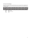
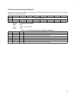
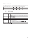
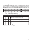
4.39 Device Control Register
The device control register is provided for PCI1130 compatibility. It contains bits that are shared between functions
0 and 1. The interrupt mode select is programmed through this register. The socket-capable force bits are also
programmed through this register. See Table 4−17 for a complete description of the register contents.
Bit 7 6 5 4 3 2 1 0
Name Device control
Type RW RW RW R RW RW RW RW
Default 0 1 1 0 0 1 1 0
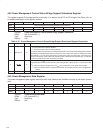
Register: Device control
Offset: 92h (Functions 0, 1)
Type: Read-only, Read/Write
Default: 66h
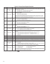
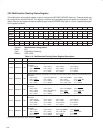
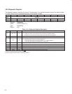
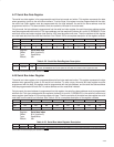
Table 4−17. Device Control Register Description
BIT SIGNAL TYPE FUNCTION
7 ‡ SKTPWR_LOCK RW
Socket power lock bit. When this bit is set to 1, software cannot power down the PC Card socket while
in D3. It may be necessary to lock socket power in order to support wake on LAN or RING if the
operating system is programmed to power down a socket when the CardBus controller is placed in the
D3 state.
6 ठ3VCAPABLE RW
3-V socket capable force bit.
0 = Not 3-V capable
1 = 3-V capable (default)
5 ‡ IO16R2 RW Diagnostic bit. This bit defaults to 1.
4 RSVD R Reserved. This bit returns 0 when read. A write has no effect.
3 ठTEST RW TI test bit. Write only 0 to this bit.
2−1 ‡§ INTMODE RW
Interrupt mode. These bits select the interrupt signaling mode. The interrupt mode bits are encoded:
00 = Parallel PCI interrupts only
01 = Reserved
10 = IRQ serialized interrupts and parallel PCI interrupts INTA
, INTB, INTC, and INTD
11 = IRQ and PCI serialized interrupts (default)
0 ठRSVD RW Reserved. Bit 0 is reserved for test purposes. Only a 0 must be written to this bit.
‡
This bit is cleared only by the assertion of GRST
.
§
These bits are global in nature and must be accessed only through function 0.