


4−36
4.49 Serial Bus Slave Address Register
The serial bus slave address register is for programmable serial bus byte read and write transactions. To write a byte,
the serial bus data register must be programmed with the data, the serial bus index register must be programmed
with the byte address, and this register must be programmed with both the 7-bit slave address and the read/write
indicator bit.
On byte reads, the byte address is programmed into the serial bus index register, this register must be programmed
with both the 7-bit slave address and the read/write indicator bit, and bit 5 (REQBUSY) in the serial bus control and
status register (see Section 4.50) must be polled until clear. Then the contents of the serial bus data register are valid
read data from the serial bus interface. See Table 4−24 for a complete description of the register contents.
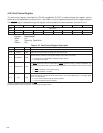
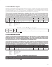
Bit 7 6 5 4 3 2 1 0
Name Serial bus slave address
Type RW RW RW RW RW RW RW RW
Default 0 0 0 0 0 0 0 0
Register: Serial bus slave address
Offset: B2h (function 0)
Type: Read/Write
Default: 00h
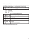
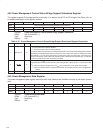
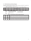
Table 4−24. Serial Bus Slave Address Register Description
BIT SIGNAL TYPE FUNCTION
7−1 ‡ SLAVADDR RW
Serial bus slave address. This bit field represents the slave address of a read or write transaction on the
serial interface.
0 ‡ RWCMD RW
Read/write command. Bit 0 indicates the read/write command bit presented to the serial bus on byte read
and write accesses.
0 = A byte write access is requested to the serial bus interface.
1 = A byte read access is requested to the serial bus interface.
‡
These bits are cleared only by the assertion of GRST
.