


7−19
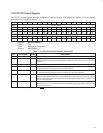
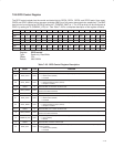
7.26 GPIO Control Register
The GPIO control register has the control and status bits for GPIO0, GPIO1, GPIO2, and GPIO3 ports. Upon reset,
GPIO0 and GPIO1 default to bus manager contender (BMC) and link power status terminals, respectively. The BMC
terminal can be configured as GPIO0 by setting bit 7 (DISABLE_BMC) to 1. The LPS terminal can be configured as
GPIO1 by setting bit 15 (DISABLE_LPS) to 1. See Table 7−23 for a complete description of the register contents.
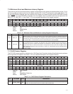
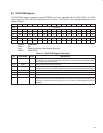
Bit 31 30 29 28 27 26 25 24 23 22 21 20 19 18 17 16
Name GPIO control
Type R R R/W R/W R R R R/W R R R/W R/W R R R R/W
Default 0 0 0 0 0 0 0 0 0 0 0 0 0 0 0 0
Bit 15 14 13 12 11 10 9 8 7 6 5 4 3 2 1 0
Name GPIO control
Type R/W R R/W R/W R R R R/W R/W R R/W R/W R R R R/W
Default 0 0 0 0 0 0 0 0 0 0 0 0 0 0 0 0
Register: GPIO control
Type: Read-only, Read/Write
Offset: FCh
Default: 0000 0000h
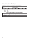
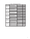
Table 7−23. GPIO Control Register Description
BIT SIGNAL TYPE FUNCTION
31−30 RSVD R Reserved. Bits 31 and 30 return 0s when read.
29 GPIO_INV3 R/W
GPIO3 polarity invert. This bit controls the input/output polarity control of GPIO3.
0 = Noninverted (default)
1 = Inverted
28 GPIO_ENB3 R/W
GPIO3 enable control. This bit controls the output enable for GPIO3.
0 = High-impedance output (default)
1 = Output is enabled
27−25 RSVD R Reserved. Bits 27−25 return 0s when read.
24 GPIO_DATA3 R/W
GPIO3 data. When GPIO3 output is enabled, the value written to this bit represents the logical data
driven to the GPIO3 terminal.
23−22 RSVD R Reserved. Bits 23 and 22 return 0s when read.
21 GPIO_INV2 R/W
GPIO2 polarity invert. This bit controls the input/output polarity control of GPIO2.
0 = Noninverted (default)
1 = Inverted
20 GPIO_ENB2 R/W
GPIO2 enable control. This bit controls the output enable for GPIO2.
0 = High-impedance output (default)
1 = Output is enabled
19−17 RSVD R Reserved. Bits 19−17 return 0s when read.
16 GPIO_DATA2 R/W
GPIO2 data. When GPIO2 output is enabled, the value written to this bit represents the logical data
driven to the GPIO2 terminal.
15 DISABLE_LPS R/W
Disable link power status (LPS). This bit configures this terminal as
0 = LPS (default)
1 = GPIO1
14 RSVD R Reserved. Bit 14 returns 0 when read.
13 GPIO_INV1 R/W
GPIO1 polarity invert. When bit 15 (DISABLE_LPS) is set to 1, this bit controls the input/output polarity
control of GPIO1.
0 = Noninverted (default)
1 = Inverted