


3−13
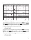
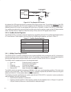
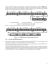
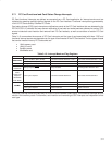
Figure 3−10 illustrates a byte read. The read protocol is very similar to the write protocol, except the R/W command
bit must be set to 1 to indicate a read-data transfer. In addition, the PCI7x21/PCI7x11 master must acknowledge
reception of the read bytes from the slave transmitter. The slave transmitter drives the SDA signal during read data
transfers. The SCL signal remains driven by the PCI7x21/PCI7x11 master.
Sb6 b4b5 b3 b2 b1 b0 0 b7 b6 b5 b4 b3 b2 b1 b0AA
Slave Address Word Address
R/W
Sb6 b4b5 b3 b2 b1 b0 1 A
Slave Address
S/P = Start/Stop ConditionM = Master Acknowledgement
b7 b6 b4b5 b3 b2 b1 b0 M P
Data Byte
Start
Restart R/W
A = Slave Acknowledgement
Stop
Figure 3−10. Serial-Bus Protocol—Byte Read
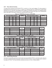
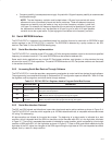
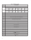
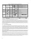
Figure 3−11 illustrates EEPROM interface doubleword data collection protocol.
S1 10 0 0 0 0 0 b7 b6 b5 b4 b3 b2 b1 b0AA
Slave Address Word Address
R/W
Data Byte 2 Data Byte 1 Data Byte 0 M PMM
M = Master Acknowledgement S/P = Start/Stop ConditionA = Slave Acknowledgement
Data Byte 3 M
S1 10 00001A
Restart
R/W
Slave Address
Start
Figure 3−11. EEPROM Interface Doubleword Data Collection
3.6.4 Serial-Bus EEPROM Application
When the PCI bus is reset and the serial-bus interface is detected, the PCI7x21/PCI7x11 controller attempts to read
the subsystem identification and other register defaults from a serial EEPROM.
This format must be followed for the PCI7x21/PCI7x11 controller to load initializations from a serial EEPROM. All bit
fields must be considered when programming the EEPROM.
The serial EEPROM is addressed at slave address 1010 000b by the PCI7x21/PCI7x11 controller. All hardware
address bits for the EEPROM must be tied to the appropriate level to achieve this address. The serial EEPROM chip
in the sample application (Figure 3−11) assumes the 1010b high-address nibble. The lower three address bits are
terminal inputs to the chip, and the sample application shows these terminal inputs tied to GND.