


2−14
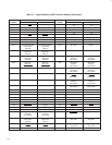
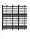
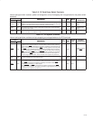
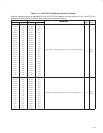
Table 2−4. Power Supply Terminals
Output description, internal pullup/pulldown resistors, and the power rail designation are not applicable for the power
supply terminals.
TERMINAL
DESCRIPTION
I/O
INPUT
EXTERNAL
PIN STRAPPING
NAME NUMBER
DESCRIPTION
I/O
TYPE
INPUT
EXTERNAL
COMPONENTS
PIN STRAPPING
(IF UNUSED)
AGND
N12, U14,
U16
Analog circuit ground terminals GND NA
AVDD
R13, R14,
V17
Analog circuit power terminals. A parallel combination of high
frequency decoupling capacitors near each terminal is suggested,
such as 0.1 µF and 0.001 µF. Lower frequency 10-µF filtering
capacitors are also recommended. These supply terminals are
separated from VDPLL_33 internal to the controller to provide
noise isolation. They must be tied to a low-impedance point on the
circuit board.
GND
0.1-µF, 0.001-µF,
and 10-µF
capacitors tied to
AGND
NA
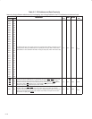
GND
G07, G08,
G13, H13,
J09, J10,
J11, K09,
K10, K11,
L08, L09,
L10, L11,
L12, M08
Digital ground terminal GND NA
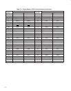
V
CC
H08, H09,
H10, H11,
H12, J08,
J12, K08,
K12, M07,
M09, M10,
M12, N07
Power supply terminal for I/O and internal voltage regulator PWR NA
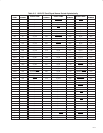
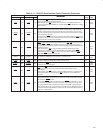
V
CCA
A05, A11
Clamp voltage for PC Card A interface. Matches card A signaling
environment, 5 V or 3.3 V
PWR Float
V
CCB
D19, K19
Clamp voltage for PC Card B interface. Matches card B signaling
environment, 5 V or 3.3 V
PWR Float
V
CCP
W03, W10 Clamp voltage for PCI and miscellaneous I/O, 5 V or 3.3 V PWR NA
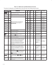
VDPLL_15 T18
1.5-V PLL circuit power terminal. An external capacitor (0.1 µF
recommended) must be placed between terminals T18 and T17
(VSSPLL) when the internal voltage regulator is enabled
(VR_EN
= 0 V). When the internal voltage regulator is disabled,
1.5-V must be supplied to this terminal and a parallel combination
of high frequency decoupling capacitors near the terminal is
suggested, such as 0.1 µF and 0.001 µF. Lower frequency 10-µF
filtering capacitors are also recommended.
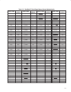
0.1-µF, 0.001-µF,
and 10-µF
capacitors tied to
VSPLL
NA
VDPLL_33 V19
3.3-V PLL circuit power terminal. A parallel combination of high
frequency decoupling capacitors near the terminal is suggested,
such as 0.1 µF and 0.001 µF. Lower frequency 10-µF filtering
capacitors are also recommended. This supply terminal is
separated from AVDD internal to the controller to provide noise
isolation. It must be tied to a low-impedance point on the circuit
board. When the internal voltage regulator is disabled
(VR_EN
= 3.3 V), no voltage is required to be supplied to this
terminal.
PWR
0.1-µF, 0.001-µF,
and 10-µF
capacitors tied to
VSPLL
NA
VR_EN H02 Internal voltage regulator enable. Active low FT FT
Pulled directly to
GND
NA
VR_PORT H01, M19 1.5-V output from the internal voltage regulator PWR
0.1-µF capacitor
tied to GND
NA
VSSPLL P14, T17
PLL circuit ground terminal. This terminal must be tied to the
low-impedance circuit board ground plane.
GND NA