


4−22
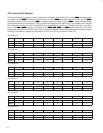
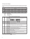
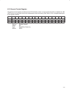
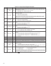
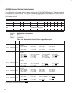
Table 4−9. General Control Register Description
BIT SIGNAL TYPE FUNCTION
15 ‡
FM_PWR_CTRL
_POL
RW
Flash media power control pin polarity. This bit controls the polarity of the MC_PWR_CTRL_0 and
MC_PWR_CTRL_1 terminals.
0 = MC_PWR_CTRL_x terminals are active low (default)
1 = MC_PWR_CTRL_x terminals are active high
14 ‡ SC_IF_SEL RWU
Smart Card interface select. This bit controls the selection of the dedicated Smart Card interface
used by the controller.
0 = EMV interface selected (default)
1 = PCI7x10-style interface selected
Note: The PCI7x10-style interface is only allowed when bits 9−8 (FM_IF_SEL field) are 01. If bits
9−8 contain any other value, then this bit is 0. Care must be taken in the design to ensure that this
bit can be set to 1 at the same time that bits 9−8 are set to 01.
13 ‡ SIM_MODE RW
When this bit is set, it reduces the query time for UltraMedia card types.
0 = Query time is unaffected (default)
1 = Query time is reduced for simulation purposes
12 ‡ IO_LIMIT_SEL RW
When this bit is set, bit 0 in the I/O limit registers (PCI offsets 30h and 38h) for both CardBus functions
is set.
0 = Bit 0 in the I/O limit registers is 0 (default)
1 = Bit 0 in the I/O limit registers is 1
11 ‡ IO_BASE_SEL RW
When this bit is set, bit 0 in the I/O base registers (PCI offsets 2Ch and 34h) for both CardBus functions
is set.
0 = Bit 0 in the I/O base registers is 0 (default)
1 = Bit 0 in the I/O base registers is 1
10 ‡ 12V_SW_SEL RW
Power switch select. This bit selects which power switch is implemented in the system.
0 = A 1.8-V capable power switch (TPS2228) is used (default)
1 = A 12-V capable power switch (TPS2226) is used
9−8 ‡ FM_IF_SEL RW
Dedicated flash media interface selection. This field controls the mode of the dedicated flash media
interface.
00 = Flash media interface configured as SD/MMC socket + MS socket (default)
01 = Flash media interface configured as 2-in-1 (SD/MMC, MS) socket
10 = Flash media interface configured as 3-in-1 (SD/MMC, MS, SM/XD) socket
11 = Reserved
7 ‡ DISABLE_SC RW When this bit is set, the Smart Card function is completely nonaccessible and nonfunctional.
6 ‡ DISABLE_SD RW When this bit is set, the SD host controller function is completely nonaccessible and nonfunctional.
5 ‡ DISABLE_FM RW When this bit is set, the flash media function is completely nonaccessible and nonfunctional.
4 ‡ DISABLE_SKTB RW When this bit is set, CardBus socket B (function 1) is completely nonaccessible and nonfunctional.
3 ‡ DISABLE_OHCI RW When this bit is set, the OHCI 1394 controller function is completely nonaccessible and nonfunctional.
2 ‡
DED_SC_PWR_
CTRL
RW
Dedicated Smart Card power control. This bit determines how power to the dedicated Smart Card
socket is controlled.
0 = Controlled through the SC_PWR_CTRL terminal (default)
1 = Controlled through the VPP voltage of socket B of the CardBus power switch (the design
must ensure that this mode can only be set when CardBus socket B is disabled).
1−0 ‡ ARB_CTRL RW
Controls top level PCI arbitration:
00 = 1394 OHCI priority 10 = Flash media/SD host priority
01 = CardBus priority 11 = Fair round robin
Note: When flash media/SD host priority is selected, there must be a two-level priority scheme with the
first level being a round robin between the flash media and SD host functions and the second level being
a round robin between the CardBus and 1394 functions.
‡
These bits are cleared only by the assertion of GRST
.