


4−1
4 PC Card Controller Programming Model
This chapter describes the PCI7x21/PCI7x11 PCI configuration registers that make up the 256-byte PCI configuration
header for each PCI7x21/PCI7x11 function. There are some bits which affect both CardBus functions, but which, in
order to work properly, must be accessed only through function 0. These are called global bits. Registers containing
one or more global bits are denoted by § in Table 4−2.
Any bit followed by a † is not cleared by the assertion of PRST
(see CardBus Bridge Power Management,
Section 3.8.10, for more details) if PME
is enabled (PCI offset A4h, bit 8). In this case, these bits are cleared only by
GRST
. If PME is not enabled, then these bits are cleared by GRST or PRST. These bits are sometimes referred to
as PME context bits and are implemented to allow PME
context to be preserved during the transition from D3
hot
or
D3
cold
to D0.
If a bit is followed by a ‡, then this bit is cleared only by GRST
in all cases (not conditional on PME being enabled).
These bits are intended to maintain device context such as interrupt routing and MFUNC programming during warm
resets.
A bit description table, typically included when the register contains bits of more than one type or purpose, indicates
bit field names, a detailed field description, and field access tags which appear in the type column. Table 4−1
describes the field access tags.
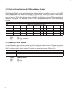
Table 4−1. Bit Field Access Tag Descriptions
ACCESS TAG NAME MEANING
R Read Field can be read by software.
W Write Field can be written by software to any value.
S Set Field can be set by a write of 1. Writes of 0 have no effect.
C Clear Field can be cleared by a write of 1. Writes of 0 have no effect.
U Update Field can be autonomously updated by the PCI7x21/PCI7x11 controller.
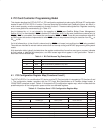
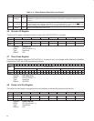
4.1 PCI Configuration Register Map (Functions 0 and 1)
The PCI7x21/PCI7x11 is a multifunction PCI device, and the PC Card controller is integrated as PCI functions 0 and
1. The configuration header, compliant with the PCI Local Bus Specification as a CardBus bridge header, is
PC99/PC2001 compliant as well. Table 4−2 illustrates the PCI configuration register map, which includes both the
predefined portion of the configuration space and the user-definable registers.
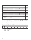
Table 4−2. Functions 0 and 1 PCI Configuration Register Map
REGISTER NAME OFFSET
Device ID Vendor ID 00h
Status ‡ Command 04h
Class code Revision ID 08h
BIST Header type Latency timer Cache line size 0Ch
CardBus socket registers/ExCA base address register 10h
Secondary status ‡ Reserved Capability pointer 14h
CardBus latency timer Subordinate bus number CardBus bus number PCI bus number 18h
CardBus memory base register 0 1Ch
CardBus memory limit register 0 20h
CardBus memory base register 1 24h
CardBus memory limit register 1 28h
‡
One or more bits in this register are cleared only by the assertion of GRST
.