


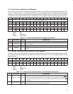


11−9
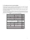
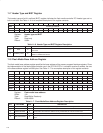
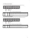
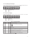
11.14 Minimum Grant Register
The minimum grant register contains the minimum grant value for the flash media controller core.
Bit 7 6 5 4 3 2 1 0
Name Minimum grant
Type RU RU RU RU RU RU RU RU
Default 0 0 0 0 0 1 1 1
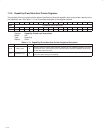
Register: Minimum grant
Offset: 3Eh
Type: Read/Update
Default: 07h
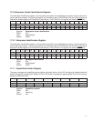
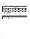
Table 11−9. Minimum Grant Register Description
BIT FIELD NAME TYPE DESCRIPTION
7−0 MIN_GNT RU
Minimum grant. The contents of this field may be used by host BIOS to assign a latency timer register value
to the flash media controller. The default for this register indicates that the flash media controller may need
to sustain burst transfers for nearly 64 µs and thus request a large value be programmed in bits 15−8 of
the PCI7x21/PCI7x11 latency timer and class cache line size register at offset 0Ch in the PCI configuration
space (see Section 11.6).
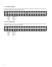
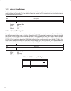
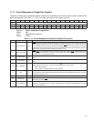
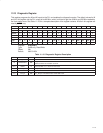
11.15 Maximum Latency Register
The maximum latency register contains the maximum latency value for the flash media controller core.
Bit 7 6 5 4 3 2 1 0
Name Maximum latency
Type RU RU RU RU RU RU RU RU
Default 0 0 0 0 0 1 0 0
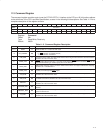
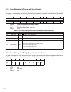
Register: Maximum latency
Offset: 3Eh
Type: Read/Update
Default: 04h
Table 11−10. Maximum Latency Register Description
BIT FIELD NAME TYPE DESCRIPTION
7−0 MAX_LAT RU
Maximum latency. The contents of this field may be used by host BIOS to assign an arbitration priority level
to the flash media controller. The default for this register indicates that the flash media controller may need
to access the PCI bus as often as every 0.25 µs; thus, an extremely high priority level is requested. The
contents of this field may also be loaded through the serial EEPROM.