


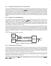

3−4
as bus master, by reading and writing PCI configuration registers. Setting bit 3 (SBDETECT) in the serial bus
control/status register (PCI offset B3h, see Section 4.50) causes the PCI7x21/PCI7x11 controller to route the SDA
and SCL signals to the SDA and SCL terminals, respectively. The read/write data, slave address, and byte addresses
are manipulated by accessing the serial bus data, serial bus index, and serial bus slave address registers (PCI offsets
B0h, B1h, and B2h; see Sections 4.47, 4.48, and 4.49, respectively).
EEPROM interface status information is communicated through the serial bus control and status register (PCI offset
B3h, see Section 4.50). Bit 3 (SBDETECT) in this register indicates whether or not the PCI7x21/PCI7x11 serial ROM
circuitry detects the pullup resistor on SCL. Any undefined condition, such as a missing acknowledge, results in bit
0 (ROM_ERR) being set. Bit 4 (ROMBUSY) is set while the subsystem ID register is loading (serial ROM interface
is busy).
The subsystem vendor ID for functions 2 and 3 is also loaded through EEPROM. The EEPROM load data goes to
all four functions from the serial EEPROM loader.
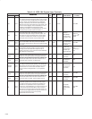
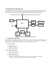
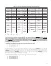
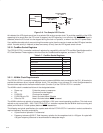
SCL
SDA
V
CC
A0
A1
A2
SCL
SDA
PCI7x21/PCI7x11
Serial
ROM
Figure 3−4. Serial ROM Application
3.4.4 Functions 0 and 1 (CardBus) Subsystem Identification
The subsystem vendor ID register (PCI offset 40h, see Section 4.26) and subsystem ID register (PCI offset 42h, see
Section 4.27) make up a doubleword of PCI configuration space for functions 0 and 1. This doubleword register is
used for system and option card (mobile dock) identification purposes and is required by some operating systems.
Implementation of this unique identifier register is a PC 99/PC 2001 requirement.
The PCI7x21/PCI7x11 controller offers two mechanisms to load a read-only value into the subsystem registers. The
first mechanism relies upon the system BIOS providing the subsystem ID value. The default access mode to the
subsystem registers is read-only, but can be made read/write by clearing bit 5 (SUBSYSRW) in the system control
register (PCI offset 80h, see Section 4.29). Once this bit is cleared, the BIOS can write a subsystem identification
value into the registers at PCI offset 40h. The BIOS must set the SUBSYSRW bit such that the subsystem vendor
ID register and subsystem ID register are limited to read-only access. This approach saves the added cost of
implementing the serial electrically erasable programmable ROM (EEPROM).
In some conditions, such as in a docking environment, the subsystem vendor ID register and subsystem ID register
must be loaded with a unique identifier via a serial EEPROM. The PCI7x21/PCI7x11 controller loads the data from
the serial EEPROM after a reset of the primary bus. Note that the SUSPEND
input gates the PCI reset from the entire
PCI7x21/PCI7x11 core, including the serial-bus state machine (see Section 3.8.6, Suspend Mode, for details on
using SUSPEND
).
The PCI7x21/PCI7x11 controller provides a two-line serial-bus host controller that can interface to a serial EEPROM.
See Section 3.6, Serial EEPROM Interface,
for details on the two-wire serial-bus controller and applications.