


3−28
• ExCA card status-change interrupt configuration register (ExCA 805h/845h, see Section 5.6): bits 3−0
• ExCA card detect and general control register (ExCA 816h/856h, see Section 5.19): bits 7, 6
• Socket event register (CardBus offset 00h, see Section 6.1): bits 3−0
• Socket mask register (CardBus offset 04h, see Section 6.2): bits 3−0
• Socket present state register (CardBus offset 08h, see Section 6.3): bits 13−7, 5−1
• Socket control register (CardBus offset 10h, see Section 6.5): bits 6−4, 2−0
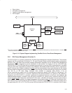
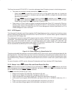
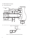
Global reset-only bits, as the name implies, are cleared only by GRST
. These bits are never cleared by PRST,
regardless of the setting of the PME enable bit. The GRST signal is gated only by the SUSPEND signal. This means
that assertion of SUSPEND
blocks the GRST signal internally, thus preserving all register contents. Figure 3−13 is
a diagram showing the application of GRST
and PRST.
The global reset-only bits (functions 0 and 1) are:
• Status register (PCI offset 06h, see Section 4.5): bits 15−11, 8
• Secondary status register (PCI offset 16h, see Section 4.14): bits 15−11, 8
• Subsystem vendor ID register (PCI offset 40h, see Section 4.26): bits 15–0
• Subsystem ID register (PCI offset 42h, see Section 4.27): bits 15–0
• PC Card 16-bit I/F legacy-mode base-address register (PCI offset 44h, see Section 4.28): bits 31−0
• System control register (PCI offset 80h, see Section 4.29): bits 31−24, 22−13, 11, 6−0
• MC_CD debounce register (PCI offset 84h, see Section 4.30): bits 7−0
• General control register (PCI offset 86h, see Section 4.31): bits 13−10, 7, 5−3, 1, 0
• General-purpose event status register (PCI offset 88h, see Section 4.32): bits 7, 6, 4−0
• General-purpose event enable register (PCI offset 89h, see Section 4.33): bits 7, 6, 4−0
• General-purpose output register (PCI offset 8Bh, see Section 4.35): bits 4−0
• Multifunction routing register (PCI offset 8Ch, see Section 4.36): bits 31−0
• Retry status register (PCI offset 90h, see Section 4.37): bits 7−5, 3, 1
• Card control register (PCI offset 91h, see Section 4.38): bits 7, 2−0
• Device control register (PCI offset 92h, see Section 4.39): bits 7−5, 3−0
• Diagnostic register (PCI offset 93h, see Section 4.40): bits 7−0
• Power management capabilities register (PCI offset A2h, see Section 4.43): bit 15
• Power management CSR register (PCI offset A4h, see Section 4.44): bits 15, 8
• Serial bus data register (PCI offset B0h, see Section 4.47): bits 7−0
• Serial bus index register (PCI offset B1h, see Section 4.48): bits 7−0
• Serial bus slave address register (PCI offset B2h, see Section 4.49): bits 7−0
• Serial bus control/status register (PCI offset B3h, see Section 4.50): bits 7, 3−0
• ExCA identification and revision register (ExCA 800h/840h, see Section 5.1): bits 7−0
• ExCA global control register (ExCA 81Eh/85Eh, see Section 5.20): bits 2−0
• CardBus socket power management register (CardBus 20h, see Section 6.6): bits 25, 24
The global reset-only bit (function 2) is:
• Subsystem vendor ID register (PCI offset 2Ch, see Section 7.12): bits 15−0
• Subsystem ID register (PCI offset 2Eh, see Section 7.12): bits 31−16
• Minimum grant and maximum latency register (PCI offset 3Eh, see Section 7.16): bits 15−0
• Power management control and status register (PCI offset 48h, see Section 7.20): bits 15, 8, 1, 0
• Miscellaneous configuration register (PCI offset F0h, see Section 7.23): bits 15, 11−8, 5−0
• Link enhancement control register (PCI offset F4h, see Section 7.24): bits 15−12, 10, 8, 7, 2, 1
• Bus options register (OHCI offset 20h, see Section 8.9): bits 15−12
• GUID high register (OHCI offset 24h, see Section 8.10): bits 31−0
• GUID low register (OHCI offset 28h, see Section 8.11): bits 31−0
• Host controller control register (OHCI offset 50h/54h, see Section 8.16): bit 23
• Link control register (OHCI offset E0h/E4h, see Section 8.31): bit 6
• PHY-link loopback test register (Local offset C14h): bits 6−4, 0
• Link test control register (Local offset C00h): bits 12−8