


11−8
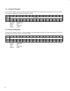
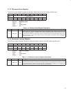
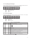
11.12 Interrupt Line Register
The interrupt line register is programmed by the system and indicates to the software which interrupt line the flash
media interface has assigned to it. The default value of this register is FFh, indicating that an interrupt line has not
yet been assigned to the function.
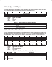
Bit 7 6 5 4 3 2 1 0
Name Interrupt line
Type RW RW RW RW RW RW RW RW
Default 1 1 1 1 1 1 1 1
Register: Interrupt line
Offset: 3Ch
Type: Read/Write
Default: FFh
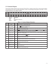
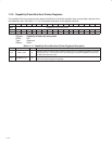
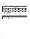
11.13 Interrupt Pin Register
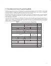
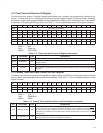
This register decodes the interrupt select inputs and returns the proper interrupt value based on Table 11−8, indicating
that the flash media interface uses an interrupt. If one of the USE_INTx terminals is asserted, the interrupt select bits
are ignored, and this register returns the interrupt value for the highest priority USE_INTx terminal that is asserted.
If bit 28, the tie-all bit (TIEALL), in the system control register (PCI offset 80h, see Section 4.29) is set to 1, then the
PCI7x21/PCI7x11 controller asserts the USE_INTA input to the flash media controller core. If bit 28 (TIEALL) in the
system control register (PCI offset 80h, see Section 4.29) is set to 0, then none of the USE_INTx inputs are asserted
and the interrupt for the flash media function is selected by the INT_SEL bits in the flash media general control register.
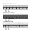
Bit 7 6 5 4 3 2 1 0
Name Interrupt pin
Type R R R R R R R R
Default 0 0 0 0 0 X X X
Register: Interrupt pin
Offset: 3Dh
Type: Read-only
Default: 0Xh
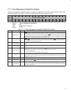
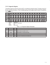
Table 11−8. PCI Interrupt Pin Register
INT_SEL BITS USE_INTA INTPIN
00 0 01h (INTA)
01 0 02h (INTB)
10 0 03h (INTC)
11 0 04h (INTD)
XX 1 01h (INTA)