


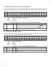

12−10
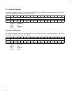
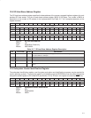
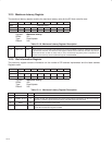
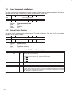
12.15 Maximum Latency Register
The maximum latency register contains the maximum latency value for the SD host controller core.
Bit 7 6 5 4 3 2 1 0
Name Maximum latency
Type RU RU RU RU RU RU RU RU
Default 0 0 0 0 0 1 0 0
Register: Maximum latency
Offset: 3Fh
Type: Read/Update
Default: 04h
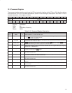
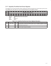
Table 12−10. Maximum Latency Register Description
BIT FIELD NAME TYPE DESCRIPTION
7−0 MAX_LAT RU Maximum latency. The contents of this field may be used by host BIOS to assign an arbitration priority level
to the SD host controller. The default for this register indicates that the SD host controller may need to
access the PCI bus as often as every 0.25 µs; thus, an extremely high priority level is requested. The
contents of this field may also be loaded through the serial EEPROM.
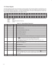
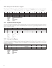
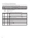
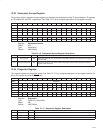
12.16 Slot Information Register
This read-only register contains information on the number of SD sockets implemented and the base address
Registers used.
Bit 7 6 5 4 3 2 1 0
Name Slot information
Type R R R R R R R R
Default 0 X X X 0 0 0 0
Register: Maximum latency
Offset: 40h
Type: Read/Update
Default: X0h
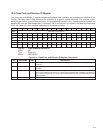
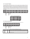
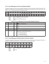
Table 12−11. Maximum Latency Register Description
BIT FIELD NAME TYPE DESCRIPTION
7 RSVD R Reserved. This bit returns 0 when read.
6−4 NUMBER_SLOTS R Number of slots. This field indicates the number of SD sockets supported by the SD host controller.
Since the controller supports three SD sockets, this field returns 010 when read.
3 RSVD R Reserved. This bit returns 0 when read.
2−0 FIRST_BAR R First base address register number. This field is hardwired to 000b to indicate that the first BAR used
for the SD host standard registers is BAR0.