


4−18
4.29 System Control Register
System-level initializations are performed through programming this doubleword register. Some of the bits are global
in nature and must be accessed only through function 0. See Table 4−8 for a complete description of the register
contents.
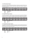
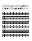
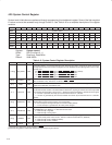
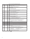
Bit 31 30 29 28 27 26 25 24 23 22 21 20 19 18 17 16
Name System control
Type RW RW RW RW RW RW RW RW R RW RW RW R R R R
Default 0 0 0 0 1 0 0 0 0 1 0 0 0 1 0 0
Bit 15 14 13 12 11 10 9 8 7 6 5 4 3 2 1 0
Name System control
Type RW RW R R R R R R R RW RW RW RW R RW RW
Default 1 0 0 1 0 0 0 0 0 1 1 0 0 0 0 0
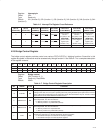
Register: System control
Offset: 80h (Functions 0, 1)
Type: Read-only, Read/Write
Default: 0844 9060h
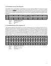
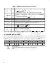
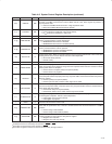
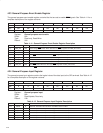
Table 4−8. System Control Register Description
BIT SIGNAL TYPE FUNCTION
31−30 ‡§ SER_STEP RW
Serial input stepping. In serial PCI interrupt mode, these bits are used to configure the serial stream PCI
interrupt frames, and can be used to accomplish an even distribution of interrupts signaled on the four PCI
interrupt slots.
00 = INTA
/INTB/INTC/INTD signal in INTA/INTB/INTC/INTD slots (default)
01 = INTA
/INTB/INTC/INTD signal in INTB/INTC/INTD/INTA slots
10 = INTA
/INTB/INTC/INTD signal in INTC/INTD/INTA/INTB slots
11 = INTA
/INTB/INTC/INTD signal in INTD/INTA/INTB/INTC slots
29 ठINTRTIE RW
This bit ties INTA to INTB internally (to INTA), and reports this through the interrupt pin register (PCI offset
3Dh, see Section 4.24). This bit has no effect on INTC
or INTD.
28 ‡ TIEALL RW
This bit ties INTA, INTB, INTC, and INTD internally (to INTA), and reports this through the interrupt pin
register (PCI offset 3Dh, see Section 4.24).
27 ‡ PSCCLK RW
P2C power switch clock. The PCI7x21/PCI7x11 CLOCK signal clocks the serial interface power switch
and the internal state machine. The default state for this bit is 0, requiring an external clock source provided
to the CLOCK terminal. Bit 27 can be set to 1, allowing the internal oscillator to provide the clock signal.
0 = CLOCK is provided externally, input to the PCI7x21/PCI7x11 controller.
1 = CLOCK is generated by the internal oscillator and driven by the PCI7x21/PCI7x11 controller.
(default)
26 ठSMIROUTE RW
SMI interrupt routing. This bit is shared between functions 0 and 1, and selects whether IRQ2 or CSC is
signaled when a write occurs to power a PC Card socket.
0 = PC Card power change interrupts are routed to IRQ2 (default).
1 = A CSC interrupt is generated on PC Card power changes.
25 ‡ SMISTATUS RW
SMI interrupt status. This socket-dependent bit is set when a write occurs to set the socket power, and
the SMIENB bit is set. Writing a 1 to this bit clears the status.
0 = SMI interrupt is signaled.
1 = SMI interrupt is not signaled.
24 ठSMIENB RW
SMI interrupt mode enable. When this bit is set, the SMI interrupt signaling generates an interrupt when
a write to the socket power control occurs. This bit is shared and defaults to 0 (disabled).
0 = SMI interrupt mode is disabled (default).
1 = SMI interrupt mode is enabled.
23 RSVD R Reserved
‡
These bits are cleared only by the assertion of GRST
.
§
These bits are global in nature and must be accessed only through function 0.