


12−1
12 SD Host Controller Programming Model
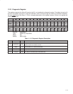
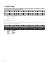
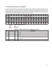
This section describes the internal PCI configuration registers used to program the PCI7x21/PCI7x11 SD host
controller interface. All registers are detailed in the same format: a brief description for each register is followed by
the register offset and a bit table describing the reset state for each register.
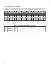
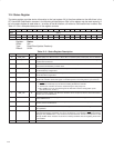
A bit description table, typically included when the register contains bits of more than one type or purpose, indicates
bit field names, a detailed field description, and field access tags which appear in the type column. Table 4−1
describes the field access tags.
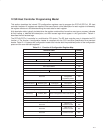
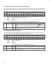
The PCI7x21/PCI7x11 controller is a multifunction PCI device. The SD host controller core is integrated as PCI
function 4. The function 4 configuration header is compliant with the PCI Local Bus Specification as a standard
header. Table 12−1 illustrates the configuration header that includes both the predefined portion of the configuration
space and the user-definable registers.
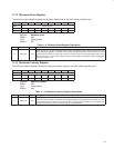
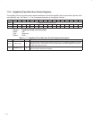
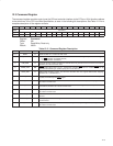
Table 12−1. Function 4 Configuration Register Map
REGISTER NAME OFFSET
Device ID Vendor ID 00h
Status Command 04h
Class code Revision ID 08h
BIST Header type Latency timer Cache line size 0Ch
Slot 0 base address 10h
Slot 1 base address 14h
Slot 2 base address 18h
Reserved 1Ch−28h
Subsystem ID ‡ Subsystem vendor ID ‡ 2Ch
Reserved 30h
Reserved
PCI power
management
capabilities pointer
34h
Reserved 38h
Maximum latency Minimum grant Interrupt pin Interrupt line 3Ch
Reserved Slot information 40h
Reserved 44h−7Ch
Power management capabilities Next item pointer Capability ID 80h
PM data
(Reserved)
PMCSR_BSE Power management control and status ‡ 84h
Reserved General control ‡ 88h
Subsystem alias 8Ch
Diagnostic ‡ 90h
Reserved
Slot 0 3.3-V
maximum current
94h
Reserved
Slot 1 3.3-V
maximum current
98h
Reserved
Slot 2 3.3-V
maximum current
9Ch
Reserved A0h−FCh
‡
One or more bits in this register are cleared only by the assertion of GRST
.