


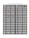


2−15
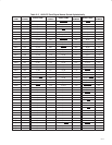
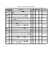
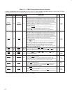
Table 2−5. PC Card Power Switch Terminals
Internal pullup/pulldown resistors, power rail designation, and pin strapping are not applicable for the power switch
terminals.
TERMINAL
DESCRIPTION
I/O
INPUT
OUTPUT
EXTERNAL
NAME NO.
DESCRIPTION
I/O
TYPE
INPUT OUTPUT
EXTERNAL
COMPONENTS
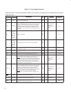
CLOCK L06
Power switch clock. Information on the DATA line is sampled at the rising edge of
CLOCK. CLOCK defaults to an input, but can be changed to an output by using bit 27
(P2CCLK) in the system control register (offset 80h, see Section 4.29).
I/O TTLI1 TTLO1
PCMCIA power
switch
DATA N01
Power switch data. DATA is used to communicate socket power control information
serially to the power switch.
O LVCO1
PCMCIA power
switch
LATCH N02
Power switch latch. LATCH is asserted by the controller to indicate to the power
switch that the data on the DATA line is valid.
O LVCO1
PCMCIA power
switch
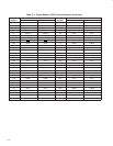
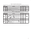
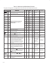
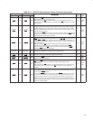
Table 2−6. PCI System Terminals
Internal pullup/pulldown resistors and pin strapping are not applicable for the PCI terminals.
TERMINAL
DESCRIPTION
I/O
INPUT
POWER
EXTERNAL
NAME NO.
DESCRIPTION
I/O
TYPE
INPUT
POWER
RAIL
EXTERNAL
COMPONENTS
GRST T01
Global reset. When the global reset is asserted, the GRST signal causes the
controller to place all output buffers in a high-impedance state and reset all internal
registers. When GRST
is asserted, the controller is completely in its default state. For
systems that require wake-up from D3, GRST
is normally asserted only during initial
boot. PRST
must be asserted following initial boot so that PME context is retained
when transitioning from D3 to D0. For systems that do not require wake-up from D3,
GRST
must be tied to PRST. When the SUSPEND mode is enabled, the controller is
protected from the GRST
, and the internal registers are preserved. All outputs are
placed in a high-impedance state, but the contents of the registers are preserved.
I LVCI2
Power-on reset or
tied to PRST
PCLK P05
PCI bus clock. PCLK provides timing for all transactions on the PCI bus. All PCI
signals are sampled at the rising edge of PCLK.
I PCII3 V
CCP
PRST
R03
PCI bus reset. When the PCI bus reset is asserted, PRST causes the controller to
place all output buffers in a high-impedance state and reset some internal registers.
When PRST
is asserted, the controller is completely nonfunctional. After PRST is
deasserted, the controller is in a default state.
When SUSPEND
and PRST are asserted, the controller is protected from PRST
clearing the internal registers. All outputs are placed in a high-impedance state, but
the contents of the registers are preserved.
I PCII3 V
CCP