


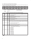

5−12
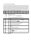
5.8 ExCA I/O Window Control Register
The ExCA I/O window control register contains parameters related to I/O window sizing and cycle timing. See
Table 5−10 for a complete description of the register contents.
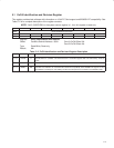
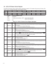
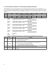
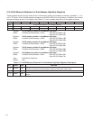
Bit 7 6 5 4 3 2 1 0
Name ExCA I/O window control
Type RW RW RW RW RW RW RW RW
Default 0 0 0 0 0 0 0 0
Register: ExCA I/O window control
Type: Read/Write
Offset: CardBus socket address + 807h: Card A ExCA offset 07h
Card B ExCA offset 47h
Default: 00h
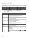
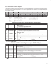
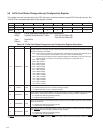
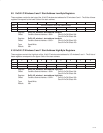
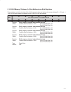
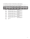
Table 5−10. ExCA I/O Window Control Register Description
BIT SIGNAL TYPE FUNCTION
7 WAITSTATE1 RW
I/O window 1 wait state. Bit 7 controls the I/O window 1 wait state for 16-bit I/O accesses. Bit 7 has no effect
on 8-bit accesses. This wait-state timing emulates the ISA wait state used by the Intel
82365SL-DF. This
bit is encoded as:
0 = 16-bit cycles have standard length (default).
1 = 16-bit cycles are extended by one equivalent ISA wait state.
6 ZEROWS1 RW
I/O window 1 zero wait state. Bit 6 controls the I/O window 1 wait state for 8-bit I/O accesses. Bit 6 has
no effect on 16-bit accesses. This wait-state timing emulates the ISA wait state used by the Intel
82365SL-DF. This bit is encoded as:
0 = 8-bit cycles have standard length (default).
1 = 8-bit cycles are reduced to equivalent of three ISA cycles.
5 IOSIS16W1 RW
I/O window 1 IOIS16 source. Bit 5 controls the I/O window 1 automatic data-sizing feature that uses IOIS16
from the PC Card to determine the data width of the I/O data transfer. This bit is encoded as:
0 = Window data width determined by DATASIZE1, bit 4 (default).
1 = Window data width determined by IOIS16.
4 DATASIZE1 RW
I/O window 1 data size. Bit 4 controls the I/O window 1 data size. Bit 4 is ignored if bit 5 (IOSIS16W1) is
set. This bit is encoded as:
0 = Window data width is 8 bits (default).
1 = Window data width is 16 bits.
3 WAITSTATE0 RW
I/O window 0 wait state. Bit 3 controls the I/O window 0 wait state for 16-bit I/O accesses. Bit 3 has no effect
on 8-bit accesses. This wait-state timing emulates the ISA wait state used by the Intel
82365SL-DF. This
bit is encoded as:
0 = 16-bit cycles have standard length (default).
1 = 16-bit cycles are extended by one equivalent ISA wait state.
2 ZEROWS0 RW
I/O window 0 zero wait state. Bit 2 controls the I/O window 0 wait state for 8-bit I/O accesses. Bit 2 has
no effect on 16-bit accesses. This wait-state timing emulates the ISA wait state used by the Intel
82365SL-DF. This bit is encoded as:
0 = 8-bit cycles have standard length (default).
1 = 8-bit cycles are reduced to equivalent of three ISA cycles.
1 IOSIS16W0 RW
I/O window 0 IOIS16 source. Bit 1 controls the I/O window 0 automatic data sizing feature that uses IOIS16
from the PC Card to determine the data width of the I/O data transfer. This bit is encoded as:
0 = Window data width is determined by DATASIZE0, bit 0 (default).
1 = Window data width is determined by IOIS16.
0 DATASIZE0 RW
I/O window 0 data size. Bit 0 controls the I/O window 0 data size. Bit 0 is ignored if bit 1 (IOSIS16W0) is
set. This bit is encoded as:
0 = Window data width is 8 bits (default).
1 = Window data width is 16 bits.