


6−1
6 CardBus Socket Registers (Functions 0 and 1)
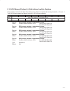
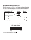
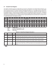
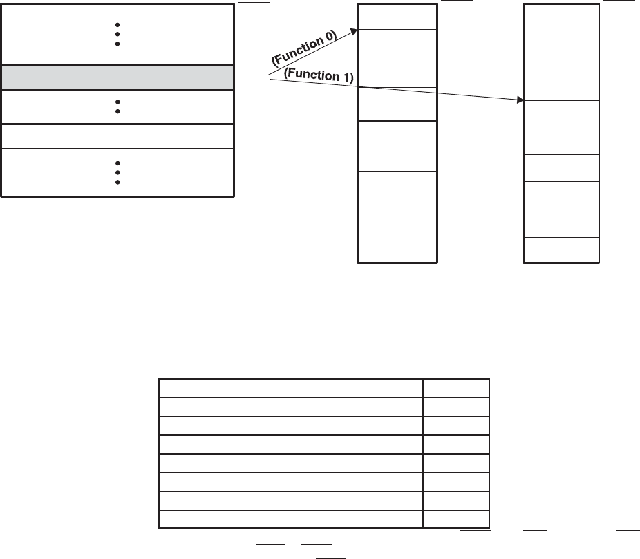
The 1997 PC Card Standard requires a CardBus socket controller to provide five 32-bit registers that report and
control socket-specific functions. The PCI7x21/PCI7x11 controller provides the CardBus socket/ExCA base address
register (PCI offset 10h, see Section 4.12) to locate these CardBus socket registers in PCI memory address space.
Each function has a separate base address register for accessing the CardBus socket registers (see Figure 6−1).
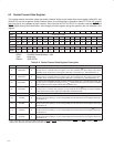
Table 6−1 gives the location of the socket registers in relation to the CardBus socket/ExCA base address.
In addition to the five required registers, the PCI7x21/PCI7x11 controller implements a register at offset 20h that
provides power management control for the socket.
16-Bit Legacy-Mode Base Address
CardBus Socket/ExCA Base Address
10h
44h
CardBus
Socket A
Registers
ExCA
Registers
Card A
20h
800h
844h
Host
Memory Space
CardBus
Socket B
Registers
ExCA
Registers
Card B
20h
800h
844h
Host
Memory Space
Note: The CardBus socket/ExCA base
address mode register is separate for
functions 0 and 1.
address register’s base address.
Offsets are from the CardBus socket/ExCA base
00h
00h
PCI7x21/PCI7x11 Configuration Registers
Offset
Offset
Offset
Figure 6−1. Accessing CardBus Socket Registers Through PCI Memory
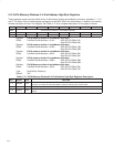
Table 6−1. CardBus Socket Registers
REGISTER NAME OFFSET
Socket event † 00h
Socket mask † 04h
Socket present state † 08h
Socket force event 0Ch
Socket control † 10h
Reserved 14h−1Ch
Socket power management ‡ 20h
†
One or more bits in the register are PME context bits and can be cleared only by the assertion of GRST
when PME is enabled. If PME is not
enabled, then these bits are cleared by the assertion of PRST
or GRST.
‡
One or more bits in this register are cleared only by the assertion of GRST
.