


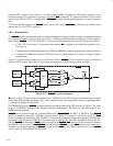
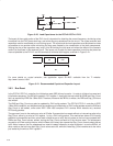

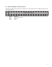

3−31
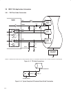
Outer Cable Shield
Chassis Ground
Figure 3−19. Non-DC Isolated Outer Shield Termination
3.9.2 Crystal Selection
The PCI7x21/PCI7x11 controller is designed to use an external 24.576-MHz crystal connected between the XI and
XO terminals to provide the reference for an internal oscillator circuit. This oscillator in turn drives a PLL circuit that
generates the various clocks required for transmission and resynchronization of data at the S100 through S400 media
data rates.
A variation of less than ±100 ppm from nominal for the media data rates is required by IEEE Std 1394-1995. Adjacent
PHYs may therefore have a difference of up to 200 ppm from each other in their internal clocks, and PHY devices
must be able to compensate for this difference over the maximum packet length. Large clock variations may cause
resynchronization overflows or underflows, resulting in corrupted packet data.
The following are some typical specifications for crystals used with the PHYs from TI in order to achieve the required
frequency accuracy and stability:
• Crystal mode of operation: Fundamental
• Frequency tolerance @ 25°C: Total frequency variation for the complete circuit is ±100 ppm. A crystal with
±30 ppm frequency tolerance is recommended for adequate margin.
• Frequency stability (over temperature and age): A crystal with ±30 ppm frequency stability is recommended
for adequate margin.
NOTE: The total frequency variation must be kept below ±100 ppm from nominal with some
allowance for error introduced by board and device variations. Trade-offs between frequency
tolerance and stability may be made as long as the total frequency variation is less than
±100 ppm. For example, the frequency tolerance of the crystal may be specified at 50 ppm and
the temperature tolerance may be specified at 30 ppm to give a total of 80 ppm possible
variation due to the crystal alone. Crystal aging also contributes to the frequency variation.
• Load capacitance: For parallel resonant mode crystal circuits, the frequency of oscillation is dependent
upon the load capacitance specified for the crystal. Total load capacitance (C
L
) is a function of not only the
discrete load capacitors, but also board layout and circuit. It is recommended that load capacitors with a
maximum of ±5% tolerance be used.
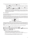
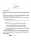
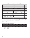
For example, load capacitors (C9 and C10 in Figure 3−20) of 16 pF each were appropriate for the layout of the
PCI7x21/PCI7x11 evaluation module (EVM), which uses a crystal specified for 12-pF loading. The load specified for
the crystal includes the load capacitors (C9 and C10), the loading of the PHY pins (C
PHY
), and the loading of the board
itself (C
BD
). The value of C
PHY
is typically about 1 pF, and C
BD
is typically 0.8 pF per centimeter of board etch; a typical
board can have 3 pF to 6 pF or more. The load capacitors C9 and C10 combine as capacitors in series so that the
total load capacitance is:
C
L
+
C9 C10
C9 ) C10
) C
PHY
) C
BD