


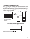

5−20
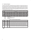
5.18 ExCA Memory Windows 0−4 Offset-Address High-Byte Registers
These registers contain the high 6 bits of the 16-bit memory window offset address for memory windows 0, 1, 2, 3,
and 4. The lower 6 bits of these registers correspond to bits A25−A20 of the offset address. In addition, the write
protection and common/attribute memory configurations are set in this register. See Table 5−13 for a complete
description of the register contents.
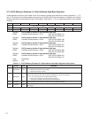
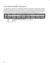
Bit 7 6 5 4 3 2 1 0
Name ExCA memory window 0−4 offset-address high-byte
Type RW RW RW RW RW RW RW RW
Default 0 0 0 0 0 0 0 0
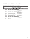
Register: ExCA memory window 0 offset-address high-byte
Offset: CardBus Socket Address + 815h: Card A ExCA Offset 15h
Card B ExCA Offset 55h
Register: ExCA memory window 1 offset-address high-byte
Offset: CardBus Socket Address + 81Dh: Card A ExCA Offset 1Dh
Card B ExCA Offset 5Dh
Register: ExCA memory window 2 offset-address high-byte
Offset: CardBus Socket Address + 825h: Card A ExCA Offset 25h
Card B ExCA Offset 65h
Register: ExCA memory window 3 offset-address high-byte
Offset: CardBus Socket Address + 82Dh: Card A ExCA Offset 2Dh
Card B ExCA Offset 6Dh
Register: ExCA memory window 4 offset-address high-byte
Offset: CardBus Socket Address + 835h: Card A ExCA Offset 35h
Card B ExCA Offset 75h
Type: Read/Write
Default: 00h
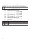
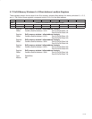
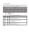
Table 5−13. ExCA Memory Windows 0−4 Offset-Address High-Byte Registers Description
BIT SIGNAL TYPE FUNCTION
7 WINWP RW
Write protect. This bit specifies whether write operations to this memory window are enabled.
This bit is encoded as:
0 = Write operations are allowed (default).
1 = Write operations are not allowed.
6 REG RW
This bit specifies whether this memory window is mapped to card attribute or common memory.
This bit is encoded as:
0 = Memory window is mapped to common memory (default).
1 = Memory window is mapped to attribute memory.
5−0 OFFHB RW
Offset-address high byte. These bits represent the upper address bits A25−A20 of the memory window offset
address.