


7−3
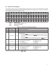
7.3 Command Register
The command register provides control over the PCI7x21/PCI7x11 interface to the PCI bus. All bit functions adhere
to the definitions in the PCI Local Bus Specification, as seen in the following bit descriptions. See Table 7−2 for a
complete description of the register contents.
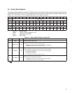
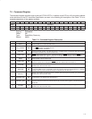
Bit 15 14 13 12 11 10 9 8 7 6 5 4 3 2 1 0
Name Command
Type R R R R R RW R RW R RW R RW R RW RW R
Default 0 0 0 0 0 0 0 0 0 0 0 0 0 0 0 0
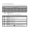
Register: Command
Offset: 04h
Type: Read/Write, Read-only
Default: 0000h
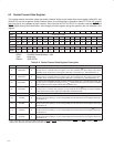
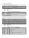
Table 7−2. Command Register Description
BIT FIELD NAME TYPE DESCRIPTION
15−11 RSVD R Reserved. Bits 15−11 return 0s when read.
10 INT_DISABLE RW
INTx disable. When set to 1, this bit disables the function from asserting interrupts on the INTx signals.
0 = INTx
assertion is enabled (default)
1 = INTx
assertion is disabled
9 FBB_ENB R
Fast back-to-back enable. The PCI7x21/PCI7x11 controller does not generate fast back-to-back
transactions; therefore, bit 9 returns 0 when read.
8 SERR_ENB RW
SERR enable. When bit 8 is set to 1, the PCI7x21/PCI7x11 SERR driver is enabled. SERR can be
asserted after detecting an address parity error on the PCI bus. The default value for this bit is 0.
7 RSVD R Reserved. Bit 7 returns 0 when read.
6 PERR_ENB RW
Parity error enable. When bit 6 is set to 1, the PCI7x21/PCI7x11 controller is enabled to drive PERR
response to parity errors through the PERR signal. The default value for this bit is 0.
5 VGA_ENB R
VGA palette snoop enable. The PCI7x21/PCI7x11 controller does not feature VGA palette snooping;
therefore, bit 5 returns 0 when read.
4 MWI_ENB RW
Memory write and invalidate enable. When bit 4 is set to 1, the PCI7x21/PCI7x11 controller is enabled
to generate MWI PCI bus commands. If this bit is cleared, then the PCI7x21/PCI7x11 controller
generates memory write commands instead. The default value for this bit is 0.
3 SPECIAL R
Special cycle enable. The PCI7x21/PCI7x11 function does not respond to special cycle transactions;
therefore, bit 3 returns 0 when read.
2 MASTER_ENB RW
Bus master enable. When bit 2 is set to 1, the PCI7x21/PCI7x11 controller is enabled to initiate cycles
on the PCI bus. The default value for this bit is 0.
1 MEMORY_ENB RW
Memory response enable. Setting bit 1 to 1 enables the PCI7x21/PCI7x11 controller to respond to
memory cycles on the PCI bus. This bit must be set to access OHCI registers. The default value for
this bit is 0.
0 IO_ENB R
I/O space enable. The PCI7x21/PCI7x11 controller does not implement any I/O-mapped functionality;
therefore, bit 0 returns 0 when read.