


8−30
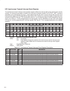
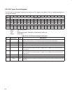
8.33 PHY Layer Control Register
The PHY layer control register reads from or writes to a PHY register. See Table 8−25 for a complete description of
the register contents.
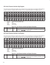
Bit 31 30 29 28 27 26 25 24 23 22 21 20 19 18 17 16
Name PHY layer control
Type RU R R R RU RU RU RU RU RU RU RU RU RU RU RU
Default 0 0 0 0 0 0 0 0 0 0 0 0 0 0 0 0
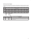
Bit 15 14 13 12 11 10 9 8 7 6 5 4 3 2 1 0
Name PHY layer control
Type RWU RWU R R RW RW RW RW RW RW RW RW RW RW RW RW
Default 0 0 0 0 0 0 0 0 0 0 0 0 0 0 0 0
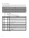
Register: PHY layer control
Offset: ECh
Type: Read/Write/Update, Read/Write, Read/Update, Read-only
Default: 0000 0000h
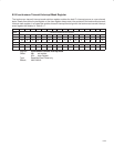
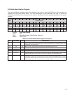
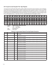
Table 8−25. PHY Control Register Description
BIT FIELD NAME TYPE DESCRIPTION
31 rdDone RU Bit 31 is cleared to 0 by the PCI7x21/PCI7x11 controller when either bit 15 (rdReg) or bit 14 (wrReg)
is set to 1. This bit is set to 1 when a register transfer is received from the PHY layer.
30−28 RSVD R Reserved. Bits 30−28 return 0s when read.
27−24 rdAddr RU This field is the address of the register most recently received from the PHY layer.
23−16 rdData RU This field is the contents of a PHY register that has been read.
15 rdReg RWU Bit 15 is set to 1 by software to initiate a read request to a PHY register, and is cleared by hardware
when the request has been sent. Bits 14 (wrReg) and 15 (rdReg) must not both be set to 1
simultaneously.
14 wrReg RWU Bit 14 is set to 1 by software to initiate a write request to a PHY register, and is cleared by hardware
when the request has been sent. Bits 14 (wrReg) and 15 (rdReg) must not both be set to 1
simultaneously.
13−12 RSVD R Reserved. Bits 13 and 12 return 0s when read.
11−8 regAddr RW This field is the address of the PHY register to be written or read. The default value for this field is 0h.
7−0 wrData RW This field is the data to be written to a PHY register and is ignored for reads. The default value for this
field is 00h.