


6−8
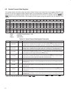
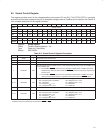
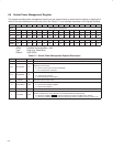
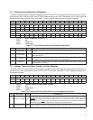
6.6 Socket Power Management Register
This register provides power management control over the socket through a mechanism for slowing or stopping the
clock on the card interface when the card is idle. See Table 6−7 for a complete description of the register contents.
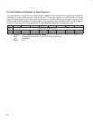
Bit 31 30 29 28 27 26 25 24 23 22 21 20 19 18 17 16
Name Socket power management
Type R R R R R R R R R R R R R R R RW
Default 0 0 0 0 0 0 0 0 0 0 0 0 0 0 0 0
Bit 15 14 13 12 11 10 9 8 7 6 5 4 3 2 1 0
Name Socket power management
Type R R R R R R R R R R R R R R R RW
Default 0 0 0 0 0 0 0 0 0 0 0 0 0 0 0 0
Register: Socket power management
Offset: CardBus Socket Address + 20h
Type: Read-only, Read/Write
Default: 0000 0000h
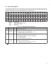
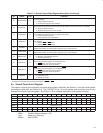
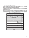
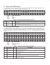
Table 6−7. Socket Power Management Register Description
BIT SIGNAL TYPE FUNCTION
31−26 RSVD R Reserved. These bits return 0s when read.
25 ‡ SKTACCES R
Socket access status. This bit provides information on whether a socket access has occurred. This bit is
cleared by a read access.
0 = No PC Card access has occurred (default).
1 = PC Card has been accessed.
24 ‡ SKTMODE R
Socket mode status. This bit provides clock mode information.
0 = Normal clock operation
1 = Clock frequency has changed.
23−17 RSVD R These bits return 0s when read.
16 CLKCTRLEN RW
CardBus clock control enable. This bit, when set, enables clock control according to bit 0 (CLKCTRL).
0 = Clock control disabled (default)
1 = Clock control enabled
15−1 RSVD R These bits return 0s when read.
0 CLKCTRL RW
CardBus clock control. This bit determines whether the CardBus CLKRUN protocol attempts to stop or
slow the CardBus clock during idle states. The CLKCTRLEN bit enables this bit.
0 = Allows the CardBus CLKRUN protocol to attempt to stop the CardBus clock (default)
1 = Allows the CardBus CLKRUN
protocol to attempt to slow the CardBus clock by a factor of 16
‡
This bit is cleared only by the assertion of GRST
.