


3−2
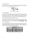
3.2 I/O Characteristics
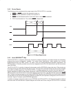
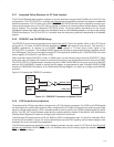
The PCI7x21/PCI7x11 controller meets the ac specifications of the PC Card Standard (release 8.1) and the PCI Local
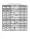
Bus Specification. Figure 3−2 shows a 3-state bidirectional buffer. Section 14.2, Recommended Operating
Conditions, provides the electrical characteristics of the inputs and outputs.
Tied for Open Drain
OE
Pad
V
CCP
Figure 3−2. 3-State Bidirectional Buffer
3.3 Clamping Voltages
The clamping voltages are set to match whatever external environment the PCI7x21/PCI7x11 controller is interfaced
with: 3.3 V or 5 V. The I/O sites can be pulled through a clamping diode to a voltage rail that protects the core from
external signals. The core power supply is 1.5 V and is independent of the clamping voltages. For example, PCI
signaling can be either 3.3 V or 5 V, and the PCI7x21/PCI7x11 controller must reliably accommodate both voltage
levels. This is accomplished by using a 3.3-V I/O buffer that is 5-V tolerant, with the applicable clamping voltage
applied. If a system designer desires a 5-V PCI bus, then V
CCP
can be connected to a 5-V power supply.
3.4 Peripheral Component Interconnect (PCI) Interface
The PCI7x21/PCI7x11 controller is fully compliant with the PCI Local Bus Specification. The PCI7x21/PCI7x11
controller provides all required signals for PCI master or slave operation, and may operate in either a 5-V or 3.3-V
signaling environment by connecting the V
CCP
terminals to the desired voltage level. In addition to the mandatory
PCI signals, the PCI7x21/PCI7x11 controller provides the optional interrupt signals INTA
, INTB, INTC, and INTD.
3.4.1 1394 PCI Bus Master
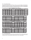
As a bus master, the 1394 function of the PCI7x21/PCI7x11 controller supports the memory commands specified in
Table 3−1. The PCI master supports the memory read, memory read line, and memory read multiple commands. The
read command usage for read transactions of greater than two data phases are determined by the selection in bits
9−8 (MR_ENHANCE field) of the PCI miscellaneous configuration register (refer to Section 7.23 for details). For read
transactions of one or two data phases, a memory read command is used.
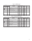
Table 3−1. PCI Bus Support
PCI
COMMAND
C/BE3
−C/BE0
OHCI MASTER FUNCTION
Memory read 0110 DMA read from memory
Memory write 0111 DMA write to memory
Memory read multiple 1100 DMA read from memory
Memory read line 1110 DMA read from memory
Memory write and invalidate 1111 DMA write to memory