


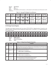

4−15
Register: Interrupt pin
Offset: 3Dh
Type: Read-only
Default: 01h (function 0), 02h (function 1), 03h (function 2), 04h (function 3), 04h (function 4), 04h
(function 5)
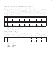
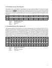
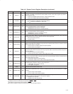
Table 4−6. Interrupt Pin Register Cross Reference
INTRTIE BIT
(BIT 29,
OFFSET 80h)
TIEALL BIT
(BIT 28,
OFFSET 80h)
INTPIN
FUNCTION 0
(CARDBUS)
INTPIN
FUNCTION 1
(CARDBUS)
INTPIN
FUNCTION 2
(1394 OHCI)
INTPIN
FUNCTION 3
(FLASH MEDIA)
INTPIN
FUNCTION 4
(SD HOST)
INTPIN
FUNCTION 5
(SMART CARD)
0 0 01h (INTA) 02h (INTB) 03h (INTC)
Determined by
bits 6−5
(INT_SEL) in the
flash media
Determined by
bits 6−5
(INT_SEL) in the
SD host general
Determined by
bits 6−5
(INT_SEL) in the
Smart Card
1 0 01h (INTA) 01h (INTA) 03h (INTC)
flash media
general control
register (see
Section 11.21)
SD host general
control register
(see
Section 12.22)
Smart Card
general control
register (see
Section 13.22)
X 1 01h (INTA) 01h (INTA) 01h (INTA) 01h (INTA) 01h (INTA) 01h (INTA)
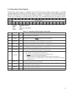
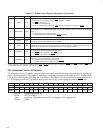
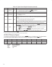
4.25 Bridge Control Register
The bridge control register provides control over various PCI7x21/PCI7x11 bridging functions. Some bits in this
register are global in nature and must be accessed only through function 0. See Table 4−7 for a complete description
of the register contents.
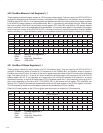
Bit 15 14 13 12 11 10 9 8 7 6 5 4 3 2 1 0
Name Bridge control
Type R R R R R RW RW RW RW RW RW R RW RW RW RW
Default 0 0 0 0 0 0 1 1 0 1 0 0 0 0 0 0
Register: Bridge control
Offset: 3Eh (Function 0, 1)
Type: Read-only, Read/Write
Default: 0340h
Table 4−7. Bridge Control Register Description
BIT
SIGNAL TYPE FUNCTION
15−11 RSVD R These bits return 0s when read.
10 POSTEN RW
Write posting enable. Enables write posting to and from the CardBus sockets. Write posting enables the
posting of write data on burst cycles. Operating with write posting disabled impairs performance on burst
cycles. Note that burst write data can be posted, but various write transactions may not. This bit is socket
dependent and is not shared between functions 0 and 1.
9 PREFETCH1 RW
Memory window 1 type. This bit specifies whether or not memory window 1 is prefetchable. This bit is
socket dependent. This bit is encoded as:
0 = Memory window 1 is nonprefetchable.
1 = Memory window 1 is prefetchable (default).
8 PREFETCH0 RW
Memory window 0 type. This bit specifies whether or not memory window 0 is prefetchable. This bit is
socket dependent. This bit is encoded as:
0 = Memory window 0 is nonprefetchable.
1 = Memory window 0 is prefetchable (default).
7 INTR RW
PCI interrupt − IREQ routing enable. This bit is used to select whether PC Card functional interrupts are
routed to PCI interrupts or to the IRQ specified in the ExCA registers.
0 = Functional interrupts are routed to PCI interrupts (default).
1 = Functional interrupts are routed by ExCA registers.