


4−20
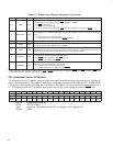
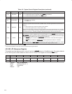
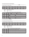
Table 4−8. System Control Register Description (continued)
BIT SIGNAL TYPE FUNCTION
4 ठCB_DPAR RW
CardBus data parity SERR signaling enable.
0 = CardBus data parity not signaled on PCI SERR
signal (default)
1 = CardBus data parity signaled on PCI SERR
signal
3 ठRSVD R Reserved. This bit returns 0 when read.
2 ‡ EXCAPOWER R
ExCA power control bit.
0 = Enables 3.3 V (default)
1 = Enables 5 V
1 ठKEEPCLK RW
Keep clock. When this bit is set, the PCI7x21/PCI7x11 controller follows the CLKRUN protocol to
maintain the system PCLK and the CCLK (CardBus clock). This bit is global to the PCI7x21/PCI7x11
functions.
0 = Allow system PCLK and CCLK clocks to stop (default)
1 = Never allow system PCLK or CCLK clock to stop
Note that the functionality of this bit has changed relative to that of the PCI12XX family of TI CardBus
controllers. In these CardBus controllers, setting this bit only maintains the PCI clock, not the CCLK.
In the PCI7x21/PCI7x11 controller, setting this bit maintains both the PCI clock and the CCLK.
0 ठRIMUX RW
PME/RI_OUT select bit. When this bit is 1, the PME signal is routed to the PME/RI_OUT terminal (R03).
When this bit is 0 and bit 7 (RIENB) of the card control register is 1, the RI_OUT
signal is routed to the
PME
/RI_OUT terminal. If this bit is 0 and bit 7 (RIENB) of the card control register is 0, then the output
is placed in a high-impedance state. This terminal is encoded as:
0 = RI_OUT
signal is routed to the PME/RI_OUT terminal if bit 7 of the card control register is 1.
(default)
1 = PME
signal is routed to the PME/RI_OUT terminal of the PCI7x21/PCI7x11 controller.
NOTE: If this bit (bit 0) is 0 and bit 7 of the card control register (PCI offset 91h, see Section 4.38) is
0, then the output on the PME
/RI_OUT terminal is placed in a high-impedance state.
‡
This bit is cleared only by the assertion of GRST
.
§
These bits are global in nature and must be accessed only through function 0.
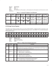
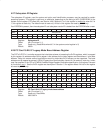
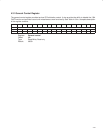
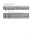
4.30 MC_CD Debounce Register
This register provides debounce time in units of 2 ms for the MC_CD signal on UltraMedia cards. This register defaults
to 19h, which gives a default debounce time of 50 ms. All bits in this register are reset by GRST
only.
Bit 7 6 5 4 3 2 1 0
Name MC_CD debounce
Type RW RW RW RW RW RW RW RW
Default 0 0 0 1 1 0 0 1
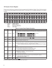
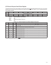
Register: MC_CD debounce
Offset: 84h (Functions 0, 1)
Type: Read/Write
Default: 19h