


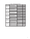

8−11
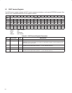
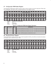
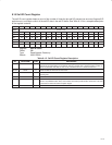
8.12 Configuration ROM Mapping Register
The configuration ROM mapping register contains the start address within system memory that maps to the start
address of 1394 configuration ROM for this node. See Table 8−8 for a complete description of the register contents.
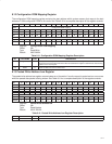
Bit 31 30 29 28 27 26 25 24 23 22 21 20 19 18 17 16
Name Configuration ROM mapping
Type RW RW RW RW RW RW RW RW RW RW RW RW RW RW RW RW
Default 0 0 0 0 0 0 0 0 0 0 0 0 0 0 0 0
Bit 15 14 13 12 11 10 9 8 7 6 5 4 3 2 1 0
Name Configuration ROM mapping
Type RW RW RW RW RW RW R R R R R R R R R R
Default 0 0 0 0 0 0 0 0 0 0 0 0 0 0 0 0
Register: Configuration ROM mapping
Offset: 34h
Type: Read/Write
Default: 0000 0000h
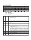
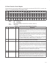
Table 8−8. Configuration ROM Mapping Register Description
BIT FIELD NAME TYPE DESCRIPTION
31−10 configROMaddr RW If a quadlet read request to 1394 offset FFFF F000 0400h through offset FFFF F000 07FFh is
received, then the low-order 10 bits of the offset are added to this register to determine the host memory
address of the read request.
9−0 RSVD R Reserved. Bits 9−0 return 0s when read.
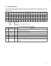
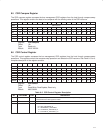
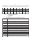
8.13 Posted Write Address Low Register
The posted write address low register communicates error information if a write request is posted and an error occurs
while the posted data packet is being written. See Table 8−9 for a complete description of the register contents.
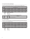
Bit 31 30 29 28 27 26 25 24 23 22 21 20 19 18 17 16
Name Posted write address low
Type RU RU RU RU RU RU RU RU RU RU RU RU RU RU RU RU
Default X X X X X X X X X X X X X X X X
Bit 15 14 13 12 11 10 9 8 7 6 5 4 3 2 1 0
Name Posted write address low
Type RU RU RU RU RU RU RU RU RU RU RU RU RU RU RU RU
Default X X X X X X X X X X X X X X X X
Register: Posted write address low
Offset: 38h
Type: Read/Update
Default: XXXX XXXXh
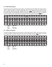
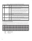
Table 8−9. Posted Write Address Low Register Description
BIT FIELD NAME TYPE DESCRIPTION
31−0 offsetLo RU The lower 32 bits of the 1394 destination offset of the write request that failed.