


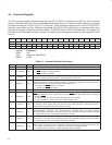

4−12
4.20 CardBus Memory Limit Registers 0, 1
These registers indicate the upper address of a PCI memory address range. They are used by the PCI7x21/PCI7x11
controller to determine when to forward a memory transaction to the CardBus bus, and likewise, when to forward a
CardBus cycle to PCI. Bits 31−12 of these registers are read/write and allow the memory base to be located anywhere
in the 32-bit PCI memory space on 4-Kbyte boundaries. Bits 11−0 are read-only and always return 0s. Writes to these
bits have no effect. Bits 8 and 9 of the bridge control register (PCI offset 3Eh, see Section 4.25) specify whether
memory windows 0 and 1 are prefetchable or nonprefetchable. The memory base register or the memory limit register
must be nonzero in order for the PCI7x21/PCI7x11 controller to claim any memory transactions through CardBus
memory windows (i.e., these windows by default are not enabled to pass the first 4 Kbytes of memory to CardBus).
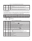
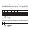
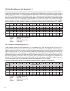
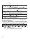
Bit 31 30 29 28 27 26 25 24 23 22 21 20 19 18 17 16
Name Memory limit registers 0, 1
Type RW RW RW RW RW RW RW RW RW RW RW RW RW RW RW RW
Default 0 0 0 0 0 0 0 0 0 0 0 0 0 0 0 0
Bit 15 14 13 12 11 10 9 8 7 6 5 4 3 2 1 0
Name Memory limit registers 0, 1
Type RW RW RW RW R R R R R R R R R R R R
Default 0 0 0 0 0 0 0 0 0 0 0 0 0 0 0 0
Register: Memory limit registers 0, 1
Offset: 20h, 28h
Type: Read-only, Read/Write
Default: 0000 0000h
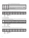
4.21 CardBus I/O Base Registers 0, 1
These registers indicate the lower address of a PCI I/O address range. They are used by the PCI7x21/PCI7x11
controller to determine when to forward an I/O transaction to the CardBus bus, and likewise, when to forward a
CardBus cycle to the PCI bus. The lower 16 bits of this register locate the bottom of the I/O window within a 64-Kbyte
page. The upper 16 bits (31−16) are all 0s, which locates this 64-Kbyte page in the first page of the 32-bit PCI I/O
address space. Bits 31−2 are read/write and always return 0s forcing I/O windows to be aligned on a natural
doubleword boundary in the first 64-Kbyte page of PCI I/O address space. Bits 1−0 are read-only, returning 00 or 01
when read, depending on the value of bit 11 (IO_BASE_SEL) in the general control register (PCI offset 86h, see
Section 4.31). These I/O windows are enabled when either the I/O base register or the I/O limit register is nonzero.
The I/O windows by default are not enabled to pass the first doubleword of I/O to CardBus.
Either the I/O base register or the I/O limit register must be nonzero to enable any I/O transactions.
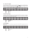
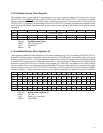
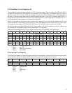
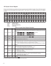
Bit 31 30 29 28 27 26 25 24 23 22 21 20 19 18 17 16
Name I/O base registers 0, 1
Type RW RW RW RW RW RW RW RW RW RW RW RW RW RW RW RW
Default 0 0 0 0 0 0 0 0 0 0 0 0 0 0 0 0
Bit 15 14 13 12 11 10 9 8 7 6 5 4 3 2 1 0
Name I/O base registers 0, 1
Type RW RW RW RW RW RW RW RW RW RW RW RW RW RW R R
Default 0 0 0 0 0 0 0 0 0 0 0 0 0 0 0 X
Register: I/O base registers 0, 1
Offset: 2Ch, 34h
Type: Read-only, Read/Write
Default: 0000 000Xh