


11−15
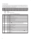
11.23 Diagnostic Register
This register programs the M and N inputs to the PLL and enables the diagnostic modes. The default values for M
and N in this register set the PLL output to be 80 MHz, which is divided to get the 40 MHz and 20 MHz needed by
the flash media cores. See Table 11−16 for a complete description of the register contents. All bits in this register are
reset by GRST
only.
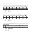
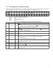
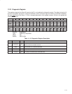
Bit 31 30 29 28 27 26 25 24 23 22 21 20 19 18 17 16
Name Diagnostic
Type R R R R R R R R R R R R R R R R/W
Default 0 0 0 0 0 0 0 0 0 0 0 0 0 0 0 0
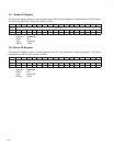
Bit 15 14 13 12 11 10 9 8 7 6 5 4 3 2 1 0
Name Diagnostic
Type R R R R R R R R/W R R R RW RW RW RW RW
Default 0 0 0 0 0 0 0 1 0 0 0 0 0 1 0 1
Register: Diagnostic
Type: Read-only, Read/Write
Offset: 54h
Default: 0000 0105h
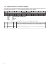
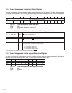
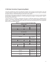
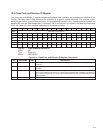
Table 11−16. Diagnostic Register Description
BIT SIGNAL TYPE FUNCTION
31−17 TBD_CTRL R PLL control bits. These bits are reserved for PLL control and test bits.
16 DIAGNOSTIC RW
Diagnostic test bit. This test bit shortens the PLL clock CLK_VALID time and shortens the card detect
debounce times for simulation and TDL.
15−11 RSVD R Reserved. Bits 15−11 return 0s when read.
10−8 PLL_N RW PLL_N input. The default value of this field is 01h.
7−5 RSVD R Reserved. Bits 7−5 return 0s when read.
4−0 PLL_M RW PLL_M input. The default value of this field is 05h.