


7−16
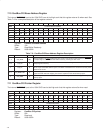
7.23 PCI Miscellaneous Configuration Register
The PCI miscellaneous configuration register provides miscellaneous PCI-related configuration. See Table 7−20 for
a complete description of the register contents.
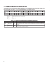
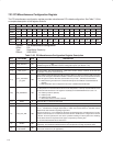
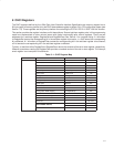
Bit 31 30 29 28 27 26 25 24 23 22 21 20 19 18 17 16
Name PCI miscellaneous configuration
Type R R R R R R R R R R R R R R R R
Default 0 0 0 0 0 0 0 0 0 0 0 0 0 0 0 0
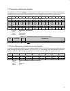
Bit 15 14 13 12 11 10 9 8 7 6 5 4 3 2 1 0
Name PCI miscellaneous configuration
Type RW R RW R RW RW RW RW R R R RW RW RW RW RW
Default 0 0 0 0 0 0 0 0 0 0 0 0 0 0 0 0
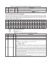
Register: PCI miscellaneous configuration
Offset: F0h
Type: Read/Write, Read-only
Default: 0000 0000h
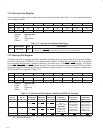
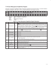
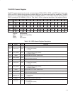
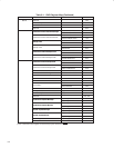
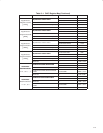
Table 7−20. PCI Miscellaneous Configuration Register Description
BIT FIELD NAME TYPE DESCRIPTION
31−16 RSVD R Reserved. Bits 31−16 return 0s when read.
15 ‡ PME_D3COLD RW
PME support from D3
cold
. This bit programs bit 15 (PME_D3COLD) in the power management
capabilities register at offset 46h in the PCI configuration space (see Section 7.19).
14−12 RSVD R Reserved. Bits 14−12 return 0s when read.
11 ‡ PCI2_3_EN RW
PCI 2.3 Enable. The PCI7x21/PCI7x11 1394 OHCI function always conforms to the PCI 2.3
specification. Therefore, this bit is tied to 0.
10 ‡
ignore_mstrIntEna
_for_pme
RW
Ignore IntMask.msterIntEnable bit for PME generation. When set, this bit causes the PME generation
behavior to be changed as described in Section 3.8. When set, this bit also causes bit 26 of the OHCI
vendor ID register at OHCI offset 40h (see Section 8.15) to read 1; otherwise, bit 26 reads 0.
0 = PME behavior generated from unmasked interrupt bits and IntMask.masterIntEnable bit
(default)
1 = PME generation does not depend on the value of IntMask.masterIntEnable
9−8 ‡ MR_ENHANCE RW
This field selects the read command behavior of the PCI master for read transactions of greater than
two data phases. For read transactions of one or two data phases, a memory read command is used.
The default of this field is 00. This register is loaded by the serial EEPROM word 12, bits 1−0.
00 = Memory read line (default)
01 = Memory read
10 = Memory read multiple
11 = Reserved, behavior reverts to default
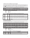
7−6 RSVD R Reserved. Bits 7−6 return 0s when read.
5 ‡ RSVD R Reserved. Bit 5 returns 0 when read.
4 ‡ DIS_TGT_ABT RW
Bit 4 defaults to 0, which provides OHCI-Lynx compatible target abort signaling. When this bit is
set to 1, it enables the no-target-abort mode, in which the PCI7x21/PCI7x11 controller returns
indeterminate data instead of signaling target abort.
The PCI7x21/PCI7x11 LLC is divided into the PCLK and SCLK domains. If software tries to access
registers in the link that are not active because the SCLK is disabled, then a target abort is issued
by the link. On some systems, this can cause a problem resulting in a fatal system error. Enabling
this bit allows the link to respond to these types of requests by returning FFh.
It is recommended that this bit be cleared to 0.
3 ‡ GP2IIC RW
When bit 3 is set to 1, the GPIO3 and GPIO2 signals are internally routed to the SCL and SDA,
respectively. The GPIO3 and GPIO2 terminals are also placed in the high-impedance state.
2 ‡
DISABLE_
SCLKGATE
RW
When bit 2 is set to 1, the internal SCLK runs identically with the chip input. This is a test feature only
and must be cleared to 0 (all applications).