


7−10
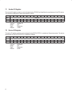
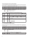
7.14 Interrupt Line Register
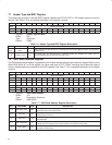
The interrupt line register communicates interrupt line routing information. See Table 7−11 for a complete description
of the register contents.
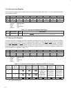
Bit 7 6 5 4 3 2 1 0
Name Interrupt line
Type RW RW RW RW RW RW RW RW
Default 1 1 1 1 1 1 1 1
Register: Interrupt line
Offset: 3Ch
Type: Read/Write
Default: FFh
Table 7−11. Interrupt Line Register Description
BIT FIELD NAME TYPE DESCRIPTION
7−0 INTR_LINE RW
Interrupt line. This field is programmed by the system and indicates to software which interrupt line the
PCI7x21/PCI7x11 PCI_INTA
is connected to. The default value for this field is 00h.
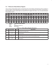
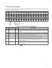
7.15 Interrupt Pin Register
The value read from this register is function dependent and depends on the values of bits 28, the tie-all bit (TIEALL),
and 29, the interrupt tie bit (INTRTIE), in the system control register (PCI offset 80h, see Section 4.29). The INTRTIE
bit is compatible with previous TI CardBus controllers, and when set to 1, ties INTB
to INTA internally. The TIEALL
bit ties INTA
, INTB, INTC, and INTD together internally. The internal interrupt connections set by INTRTIE and TIEALL
are communicated to host software through this standard register interface. This read-only register is described for
all PCI7x21/PCI7x11 functions in Table 7−12.
Bit 7 6 5 4 3 2 1 0
Name Interrupt pin
Type R R R R R R R R
Default 0 0 0 0 0 0 1 0
Register: Interrupt pin
Offset: 3Dh
Type: Read-only
Default: 02h
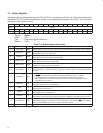
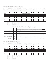
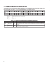
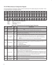
Table 7−12. PCI Interrupt Pin Register—Read-Only INTPIN Per Function
INTRTIE BIT
(BIT 29,
OFFSET 80h)
TIEALL BIT
(BIT 28,
OFFSET 80h)
INTPIN
FUNCTION 0
(CARDBUS)
INTPIN
FUNCTION 1
(CARDBUS)
INTPIN
FUNCTION 2
(1394 OHCI)
INTPIN
FUNCTION 3
(FLASH MEDIA)
INTPIN
FUNCTION 4
(SD HOST)
INTPIN
FUNCTION 5
(SMART CARD)
0 0 01h (INTA) 02h (INTB) 03h (INTC)
Determined by
bits 6−5
(INT_SEL) in the
flash media
Determined by
bits (INT_SEL) in
the SD host
Determined by
bits (INT_SEL) in
the Smart Card
1 0 01h (INTA) 01h (INTA) 03h (INTC)
flash media
general control
register (see
Section 11.21)
the SD host
general control
register (see
Section 12.22)
the Smart Card
general control
register (see
Section 13.22)
X 1 01h (INTA) 01h (INTA) 01h (INTA) 01h (INTA) 01h (INTA) 01h (INTA)
NOTE: When configuring the PCI7x21/PCI7x11 functions to share PCI interrupts, multifunction terminal MFUNC3 must be configured as IRQSER
prior to setting the INTRTIE bit.