


Page 106 Epson Research and Development
Vancouver Design Center
S1D13708 Hardware Functional Specification
X39A-A-001-02 Issue Date: 02/03/07
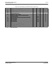
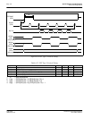
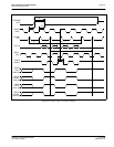
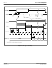
1. Ts = pixel clock period
2. t1typ = ((REG[12h] bits 6-0) + 1) x 8
3. t2typ = (REG[20h] bits 6-0) + 1
4. t3typ = (REG[17h] bits 1-0, REG[16h] bits 7-0) + 3
5. t8typ = (REG[14h] bits 6-0) x 8
6. t9typ = ((REG[D5h] bits 7-0) x 2
7. t10typ = ((REG[D6h] bits 7-0) x 2
8. t11typ = ((REG[D7h] bits 7-0) x 2
9. t12typ = ((REG[D8h] bits 7-0) x 2
10. t14typ = ((REG[D9h] bits 7-0) x 2
Note
When TFT type 3 panel interface is selected, the following formula must be satisfied.
HTP - (HDS + HDP) > (Number of Source Driver IC * 3) + 3
Note
When REG[D6h] = 0, GPIO1 (OE) pulse width equals FPLINE (LP) pulse width.
Note
When REG[D9h] = 0, t13 = 4ns and GPIO0 (CPV) pulse width equals FPLINE (LP)
pulse width.
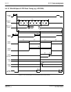
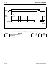
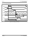
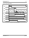
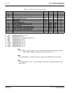
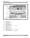
Table 6-38: TFT Type 3 Horizontal Timing
Symbol Parameter Min Typ Max Units
t1
Horizontal total period 8 note 2 1024 Ts (note 1)
t2
FPLINE pulse width 1 note 3 256 Ts
t3
FPLINE rising edge to GPIO3 rising edge note 4 Ts
t4 GPIO3 pulse width Ts
t5
GPIO3 rising edge to 1st data 1 Ts
t6
Data setup time 0.5 Ts
t7
Data hold time 0.5 Ts
t8
Horizontal display period 8 note 5 1024 Ts
t9 FPLINE rising edge to GPIO1 rising edge 0 note 6 512 Ts
t10 GPIO1 pulse width 2 note 7 512 Ts
t11 FPLINE rising edge to GPIO2 toggle position 0 note 8 512 Ts
t12 FPLINE rising edge to GPIO4 toggle position 0 note 9 512 Ts
t13 FPLINE rising edge to GPIO0 rising edge 0 Ts
t14 GPIO0 pulse width 2 note 10 512 Ts