


Page 40 Epson Research and Development
Vancouver Design Center
S1D13708 Hardware Functional Specification
X39A-A-001-02 Issue Date: 02/03/07
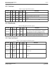
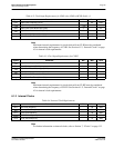
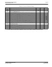
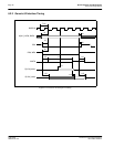
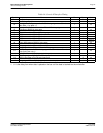
4.6 LCD Interface Pin Mapping
Note
1
GPIO pins must be configured as outputs (CNF3 = 0 at RESET#) when TFT-Type 2,
TFT-Type 3, HR-TFT or D-TFD panels are selected.
2
These pin mappings use signal names commonly used for each panel type, however
signal names may differ between panel manufacturers. The values shown in brackets
represent the color components as mapped to the corresponding FPDATxx signals at
the first valid edge of FPSHIFT. For further FPDATxx to LCD interface mapping, see
Section 6.4, “Display Interface” on page 68.
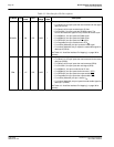
Table 4-10: LCD Interface Pin Mapping
Pin Name
Monochrome Passive
Panel
Color Passive Panel Color TFT Panel
Single
Single
Generic TFT (TFT Type 1)
Sharp HR-
TFT
1
Epson
D-TFD
1
TFT Type 2 TFT Type 3 TFT Type 4
4-bit
Format 1
8-bit
Format 2
8-bit
16-Bit
4-bit 8-bit 9-bit 12-bit 18-bit 18-bit 18-bit 18-bit 18-bit 18-bit
FPFRAME FPFRAME SPS DY STV STV FPFRAME
FPLINE FPLINE LP LP STB LP FPLINE
FPSHIFT FPSHIFT DCLK XSCL CLK CPH FPSHIFT
DRDY MOD FPSHIFT2 MOD DRDY
no connect GCP INV INV DRDY
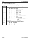
FPDAT0
driven 0 D0 driven 0 D0 (B5)
2
D0 (G3)
2
D0 (R6)
2
R2 R3 R5 R5 R5 R5 R5 R5
FPDAT1
driven 0 D1 driven 0 D1 (R5)
2
D1 (R3)
2
D1 (G5)
2
R1 R2 R4 R4 R4 R4 R4 R4
FPDAT2
driven 0 D2 driven 0 D2 (G4)
2
D2 (B2)
2
D2 (B4)
2
R0 R1 R3 R3 R3 R3 R3 R3
FPDAT3
driven 0 D3 driven 0 D3 (B3)
2
D3 (G2)
2
D3 (R4)
2
G2 G3 G5 G5 G5 G5 G5 G5
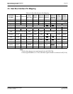
FPDAT4 D0 D4 D0 (R2)
2
D4 (R3)
2
D4 (R2)
2
D8 (B5)
2
G1 G2 G4 G4 G4 G4 G4 G4
FPDAT5 D1 D5 D1 (B1)
2
D5 (G2)
2
D5 (B1)
2
D9 (R5)
2
G0 G1 G3 G3 G3 G3 G3 G3
FPDAT6 D2 D6 D2 (G1)
2
D6 (B1)
2
D6 (G1)
2
D10 (G4)
2
B2 B3 B5 B5 B5 B5 B5 B5
FPDAT7 D3 D7 D3 (R1)
2
D7 (R1)
2
D7 (R1)
2
D11 (B3)
2
B1 B2 B4 B4 B4 B4 B4 B4
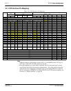
FPDAT8
driven 0 driven 0 driven 0 driven 0 driven 0 D4 (G3)
2
B0 B1 B3 B3 B3 B3 B3 B3
FPDAT9
driven 0 driven 0 driven 0 driven 0 driven 0 D5 (B2)
2
driven 0 R0 R2 R2 R2 R2 R2 R2
FPDAT10
driven 0 driven 0 driven 0 driven 0 driven 0 D6 (R2)
2
driven 0 driven 0 R1 R1 R1 R1 R1 R1
FPDAT11
driven 0 driven 0 driven 0 driven 0 driven 0 D7 (G1)
2
driven 0 driven 0 R0 R0 R0 R0 R0 R0
FPDAT12
driven 0 driven 0 driven 0 driven 0 driven 0 D12 (R3)
2
driven 0 G0 G2 G2 G2 G2 G2 G2
FPDAT13
driven 0 driven 0 driven 0 driven 0 driven 0 D13 (G2)
2
driven 0 driven 0 G1 G1 G1 G1 G1 G1
FPDAT14
driven 0 driven 0 driven 0 driven 0 driven 0 D14 (B1)
2
driven 0 driven 0 G0 G0 G0 G0 G0 G0
FPDAT15
driven 0 driven 0 driven 0 driven 0 driven 0 D15 (R1)
2
driven 0 B0 B2 B2 B2 B2 B2 B2
FPDAT16
driven 0 driven 0 driven 0 driven 0 driven 0 driven 0 driven 0 driven 0 B1 B1 B1 B1 B1 B1
FPDAT17
driven 0 driven 0 driven 0 driven 0 driven 0 driven 0 driven 0 driven 0 B0 B0 B0 B0 B0 B0
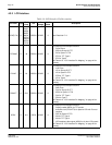
GPIO0 GPIO0 GPIO0 GPIO0 GPIO0 GPIO0 GPIO0 GPIO0 GPIO0 GPIO0 PS XINH VCLK CPV GPIO0
GPIO1 GPIO1 GPIO1 GPIO1 GPIO1 GPIO1 GPIO1 GPIO1 GPIO1 GPIO1 CLS YSCL AP OE GPIO1
GPIO2 GPIO2 GPIO2 GPIO2 GPIO2 GPIO2 GPIO2 GPIO2 GPIO2 GPIO2 REV FR POL POL GPIO2
GPIO3 GPIO3 GPIO3 GPIO3 GPIO3 GPIO3 GPIO3 GPIO3 GPIO3 GPIO3 SPL FRS STH EIO GPIO3
GPIO4 GPIO4 GPIO4 GPIO4 GPIO4 GPIO4 GPIO4 GPIO4 GPIO4 GPIO4
GPIO4
(output only)
RES
GPIO4
(output only)
VCOM GPIO4
GPIO5 GPIO5 GPIO5 GPIO5 GPIO5 GPIO5 GPIO5 GPIO5 GPIO5 GPIO5
GPIO5
(output only)
DD_P1
GPIO5
(output only)
XOEV GPIO5
GPIO6 GPIO6 GPIO6 GPIO6 GPIO6 GPIO6 GPIO6 GPIO6 GPIO6 GPIO6
GPIO6
(output only)
YSCLD
GPIO6
(output only)
CMD GPIO6
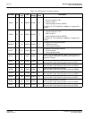
GPO0 GPO0 (General Purpose Output) MOD GPO0 GPO0 GPO0 GPO0
GPO1 GPO1 GPO1 PCLK1 GPO1
GPO2 GPO2 GPO2 PCLK2 GPO2
GPO3 GPO3 GPO3 XRESH GPO3
GPO4 GPO4 GPO4 XRESV GPO4
GPO5 GPO5 GPO5 XOHV GPO5
GPO6 GPO6 GPO6 XSTBY GPO6
GPO7 GPO7 GPO7 PMDE GPO7
CVOUT CVOUT CVOUT CVOUT CVOUT
PWMOUT PWMOUT PWMOUT PWMOUT PWMOUT