Page 44 Epson Research and Development
Vancouver Design Center
S1D13708 Hardware Functional Specification
X39A-A-001-02 Issue Date: 02/03/07
6.2 CPU Interface Timing
The following section includes CPU interface AC Timing. These timings are based on IO
V
DD
= 3.3V and Core V
DD
= 1.8V.
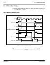
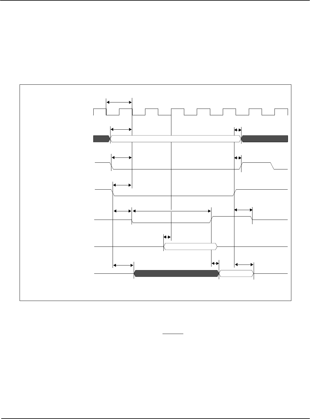
6.2.1 Generic #1 Interface Timing
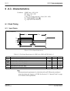
Figure 6-2 Generic #1 Interface Timing
Note
The above diagram assumes that WAIT# is used and that MCLK = BCLK.
T
CLK
t3
t5
t8
t9
CLK
A[16:1], M/R#
CS#
WE0#, WE1#, RD0#, RD1#
WAIT#
D[15:0] (write)
D[15:0] (read)
t13
t7
t11
t14
t15
t10
t6
t4


