


Page 36 Epson Research and Development
Vancouver Design Center
S1D13708 Hardware Functional Specification
X39A-A-001-02 Issue Date: 02/03/07
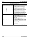
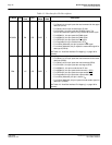
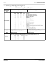
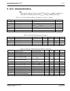
GPIO5 IO L10 PBCC8 IOVDD 0
This pin has multiple functions.
• DD_P1 for Epson D-TFD
• XOEV for Type 3
• General purpose IO pin 5 (GPIO5)
See Table 4-10: “LCD Interface Pin Mapping,” on page 40
for
summary.
GPIO6 IO K9 PBCC8 IOVDD 0
This pin has multiple functions.
• YSCLD for Epson D-TFD
• CMD for Type 3
• General purpose IO pin 6 (GPIO6)
See Table 4-10: “LCD Interface Pin Mapping,” on page 40
for
summary.
PWMOUT O H9 PBCC8 IOVDD 0
This output pin has multiple functions.
• PWM Clock output
• General purpose output
CVOUT O G11 PBCC8 IOVDD 0
This output pin has multiple functions.
• CV Pulse Output
• General purpose output
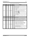
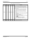
GPO0 O D11 POC8 IOVDD 0
General Purpose Output (possibly used for controlling the LCD
power). It may also be used for the MOD control signal of the
Sharp HR-TFT panel.
GPO1 O E9 POC8 IOVDD 0
General Purpose Output pin 1 (GPO1).
When used with a Type 3 panel this pin functions as PCLK1.
GPO2 O F8 POC8 IOVDD 0
General Purpose Output pin 2 (GPO2).
When used with a Type 3 panel this pin functions as PCLK2.
GPO3 O E10 POC8 IOVDD 0
General Purpose Output pin 3 (GPO3).
When used with a Type 3 panel this pin functions as XRESH.
GPO4 O E11 POC8 IOVDD 0
General Purpose Output pin 4 (GPO4).
When used with a Type 3 panel this pin functions as XRESV.
GPO5 O F9 POC8 IOVDD 0
General Purpose Output pin 5 (GPO5).
When used with a Type 3 panel this pin functions as XOHV.
GPO6 O G8 POC8 IOVDD 0
General Purpose Output pin 6 (GPO6).
When used with a Type 3 panel this pin functions as XSTBY.
GPO7 O F10 POC8 IOVDD 0
General Purpose Output pin 7 (GPO7).
When used with a Type 3 panel this pin functions as PMDE.
Table 4-4: LCD Interface Pin Descriptions
Pin Name Type
PFBGA
Pin #
Cell
IO
Voltage
RESET#
State
Description