


Epson Research and Development Page 15
Vancouver Design Center
Interfacing to the Motorola MPC821 Microprocessor S1D13708
Issue Date: 01/11/06 X39A-G-009-01
4 MPC821 to S1D13708 Interface
4.1 Hardware Description
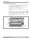
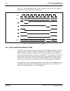
The interface between the S1D13708 and the MPC821 requires no external glue logic. The
polarity of the WAIT# signal must be selected as active high by connecting CNF5 to IO
V
DD
(see Table 4-2:, “Summary of Power-On/Reset Configuration Options,” on page 18).
BS# (bus start) is not used in this implementation and must be tied high (connected to IO
V
DD
).
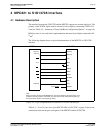
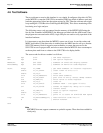
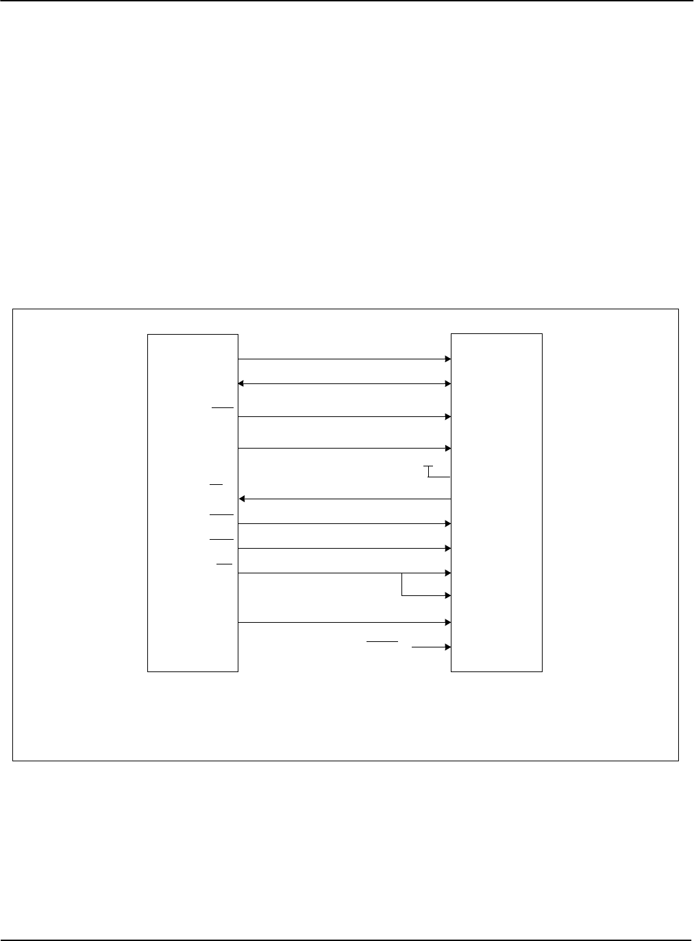
The following diagram shows a typical implementation of the MPC821 to S1D13708
interface.
Figure 4-1: Typical Implementation of MPC821 to S1D13708 Interface
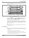
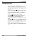
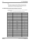
Table 4-1:, “List of Connections from MPC821ADS to S1D13708” on page 16 shows the
connections between the pins and signals of the MPC821 and the S1D13708.
MPC821
S1D13708
A[15:31]
D[0:15]
CS4
TA
WE0
WE1
OE
SYSCLK
AB[16:0]
DB[15:0]
CS#
WAIT#
WE1#
WE0#
RD/WR#
RD#
CLKI
RESET#
BS#
System RESET
Note:
When connecting the S1D13708 RESET# pin, the system designer should be aware of all
conditions that may reset the S1D13708 (e.g. CPU reset can be asserted during wake-up
from power-down modes, or during debug states).
M/R#
A14
IO V
DD