


Epson Research and Development Page 19
Vancouver Design Center
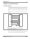
Interfacing to the Motorola MPC821 Microprocessor S1D13708
Issue Date: 01/11/06 X39A-G-009-01
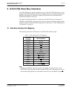
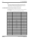
4.5 MPC821 Chip Select Configuration
Chip select 4 is used to control the S1D13708. The following options are selected in the
base address register (BR4).
• BA (0:16) = 0000 0000 0100 0000 0 – set starting address of S1D13708 to 40 0000h
• AT (0:2) = 0 – ignore address type bits.
• PS (0:1) = 1:0 – memory port size is 16 bits
• PARE = 0 – disable parity checking
• WP = 0 – disable write protect
• MS (0:1) = 0:0 – select General Purpose Chip Select module to control this chip select
• V = 1 – set valid bit to enable chip select
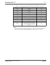
The following options were selected in the option register (OR4).
• AM (0:16) = 1111 1111 1100 0000 0 – mask all but upper 10 address bits; S1D13708
consumes 4M byte of address space
• ATM (0:2) = 0 – ignore address type bits
• CSNT = 0 – normal CS
/WE negation
• ACS (0:1) = 1:1 – delay CS
assertion by ½ clock cycle from address lines
• BI = 1 – assert Burst Inhibit
• SCY (0:3) = 0 – wait state selection; this field is ignored since external transfer
acknowledge is used; see SETA below
• SETA = 1 – the S1D13708 generates an external transfer acknowledge using the
WAIT# line
• TRLX = 0 – normal timing
• EHTR = 0 – normal timing