


Page 152 Epson Research and Development
Vancouver Design Center
S1D13708 Hardware Functional Specification
X39A-A-001-02 Issue Date: 02/03/07
bits 7-4 PWM Clock Divide Select Bits [3:0]
The value of these bits represents the power of 2 by which the selected PWM clock source
is divided.
Note
This divided clock is further divided by 256 before it is output at PWMOUT.
bits 3-1 CV Pulse Divide Select Bits [2:0]
The value of these bits represents the power of 2 by which the selected CV Pulse source is
divided.
Note
This divided clock is further divided by 2 before it is output at the CVOUT.
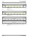
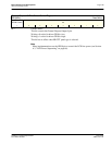
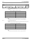
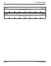
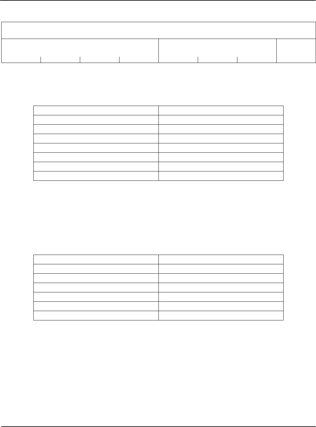
PWM Clock / CV Pulse Configuration Register
REG[B1h] Read/Write
PWM Clock Divide Select Bits 3-0 CV Pulse Divide Select Bits 2-0
PWMCLK
Source Select
76543210
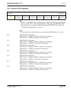
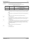
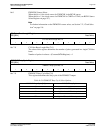
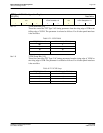
Table 8-17: PWM Clock Divide Select Options
PWM Clock Divide Select Bits [3:0] PWM Clock Divide Amount
0h 1
1h 2
2h 4
3h 8
... ...
Ch 4096
Dh-Fh Reserved
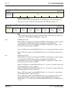
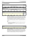
Table 8-18: CV Pulse Divide Select Options
CV Pulse Divide Select Bits [2:0] CV Pulse Divide Amount
0h 1
1h 2
2h 4
3h 8
... ...
7h 128