


Page 14 Epson Research and Development
Vancouver Design Center
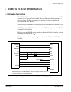
S1D13708 Interfacing to the NEC VR4181A™ Microprocessor
X39A-G-008-01 Issue Date: 01/11/05
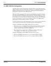
4.3 NEC VR4181A Configuration
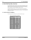
The S1D13708 is a memory mapped device. The S1D13708 uses two 128K byte blocks
which are selected using A17 from the NEC VR181A (A17 is connected to the S1D13708
M/R# pin).The internal registers occupy the first 128K bytes block and the 80K byte
display buffer occupies the second 128K byte block.
When the VR4181A embedded LCD controller is disabled, the external LCD controller
chip select signal (#LCDCS) decodes either a 64K byte, 128K byte, 256K byte, or 512K
byte memory block in the VR4181A external ISA memory. The S1D13708 requires this
block of memory to be set to 256K bytes. With this configuration, the S1D13708 internal
registers starting address is located at physical memory location 133C_0000h and the
display buffer is located at memory location 133E_0000h.
The NEC VR4181A must be configured through its internal registers to map the S1D13708
to the external LCD controller space. The following register values must be set.
• Register LCDGPMD at address 0B00_032Eh must be set as follows.
• Bit 7 must be set to 1 to disable the internal LCD controller and enable the external
LCD controller interface. Disabling the internal LCD controller also maps pin
SHCLK to #LCDCS and pin LOCLK to #MEMCS16.
• Bits [1:0] must be set to 10b to reserve 256Kbytes of memory address range,
133C_0000h to 133F_FFFFh for the external LCD controller.
• Register GPMD2REG at address 0B00_0304h must be set as follows.
• Bits [9:8] (GP20MD[1:0]) must be set to 11’b to map pin GPIO20 to #UBE.
• Bits [5:4] (GP18MD[1:0]) must be set to 01’b to map pin GPIO18 to IORDY.