


Page 8 Epson Research and Development
Vancouver Design Center
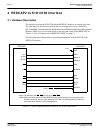
S1D13708 Interfacing to the Motorola RedCap2
X39A-G-014-01 Issue Date: 01/11/06
2 Interfacing to the REDCAP2
2.1 The REDCAP2 System Bus
REDCAP2 integrates a RISC microprocessor (MCU) and a general purpose digital signal
processor (DSP) on a single chip. The External Interface Module (EIM) handles the
interface to external devices. This section provides an overview of the operation of the
REDCAP2 bus in order to establish interface requirements.
2.2 Overview
REDCAP2 uses a 22-bit address bus (A[21:0]) and 16-bit data bus (D[15:0]). All IO is
synchronous to a square wave reference clock called CKO. The CKO source can be the
DSP clock or the MCU clock and is selected/disabled in the Clock Control Register
(CKCTL).
REDCAP2 can generate up to 6 independent chip select outputs. Each chip select has a
memory range of 16M bytes and can be independently programmed for wait-states and port
size.
Note
REDCAP2 does not provide a wait or termination acknowledge signal to external devic-
es. Therefore, all external devices must guarantee a fixed cycle length.
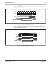
2.3 Bus Transactions
The chip initiates a data transfer by placing the memory address on address lines A0
through A21. Several control signals are provided with the memory address.
•R/W
— set high for read cycles and low for write cycles.
•EB0
— active low signal indicates access to data byte 0 (D[15:8]) during read or write
cycles.
•EB1
— active low signal indicates access to data byte 1 (D[7:0]) during read or write
cycles.
•OE
— active low signal indicates read accesses and enables slave devices to drive the
data bus.