


Epson Research and Development Page 61
Vancouver Design Center
Hardware Functional Specification S1D13708
Issue Date: 02/03/07 X39A-A-001-02
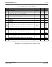
1. t12 is the delay from when data is placed on the bus until the data is latched into the write buffer.
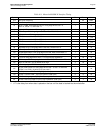
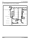
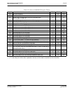
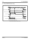
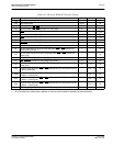
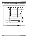
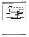
Table 6-13: Motorola DragonBall Interface without DTACK Timing
Symbol Parameter
MC68EZ328 MC68VZ328
Unit
Min Max Min Max
f
CLKO
Bus Clock frequency 16 33 MHz
T
CLKO
Bus Clock period
1/f
CLKO
1/f
CLKO
ns
t3
A[16:0] setup 1st CLKO when CSX = 0 and either UWE/LWE
or OE
= 0
00ns
t4 A[16:0] hold from CSX rising edge 0 0 ns
t5a
CSX asserted for MCLK = BCLK
(CPU wait state register should be programmed to 4 wait
states)
77T
CLKO
t5b
CSX
asserted for MCLK = BCLK ÷ 2
(CPU wait state register should be programmed to 8 wait
states)
Not Supported
11 T
CLKO
t5c
CSX
asserted for MCLK = BCLK ÷ 3
(CPU wait state register should be programmed to 10 wait
states)
Not Supported
13 T
CLKO
t6 CSX setup to CLKO rising edge 2 2 ns
t7 CSX
rising edge setup to CLKO rising edge 2 2 ns
t8 UWE/LWE setup to CLKO rising edge 2 2 ns
t9 UWE/LWE rising edge to CSX rising edge 0 0 ns
t10 OE
setup to CLKO rising edge 2 2 ns
t11 OE hold from CSX rising edge 0 0 ns
t12
D[15:0] setup to 3rd CLKO after CSX, UWE/LWE asserted
(write cycle) (see note 1)
11ns
t13 CSX
rising edge to D[15:0] output Hi-Z (write cycle) 0 0 ns
t14 Falling edge of OE to D[15:0] driven (read cycle) 5 11 5 11 ns
t15a
1st CLKO rising edge after OE
and CSX asserted low to
D[15:0] valid for MCLK = BCLK (read cycle)
6T
CLKO
+ 6 6T
CLKO
+ 6
ns
t15b
1st CLKO rising edge after OE
and CSX asserted low to
D[15:0] valid for MCLK = BCLK ÷ 2 (read cycle)
Not Supported
9T
CLKO
+ 6
ns
t15c
1st CLKO rising edge after OE and CSX asserted low to
D[15:0] valid for MCLK = BCLK ÷ 3 (read cycle)
Not Supported
12T
CLKO
+ 6
ns
t16 CSX rising edge to D[15:0] output Hi-Z (read cycle) 3 9 3 9 ns