


Page 30 Epson Research and Development
Vancouver Design Center
S1D13708 Hardware Functional Specification
X39A-A-001-02 Issue Date: 02/03/07
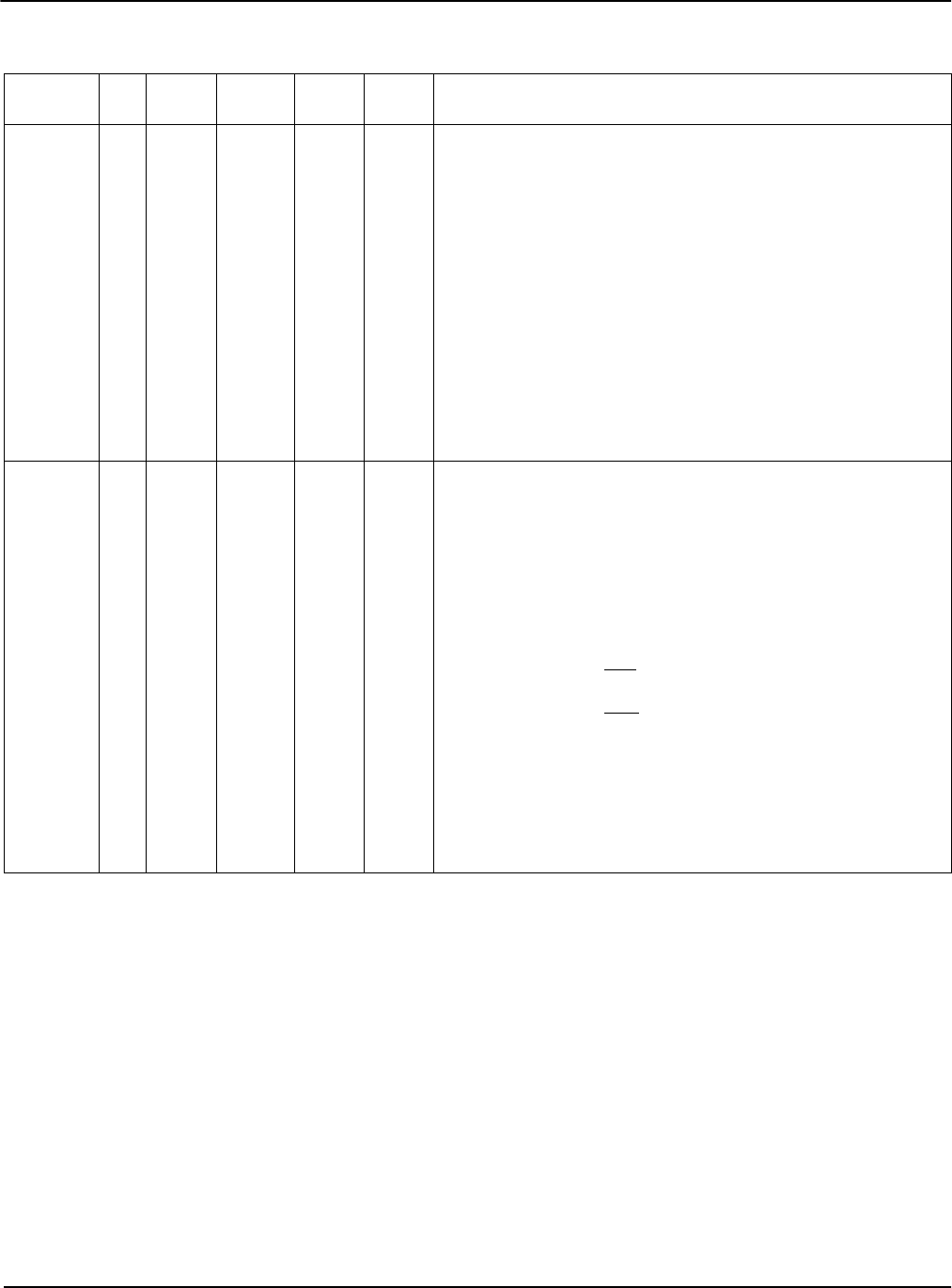
DB[15:0] IO
C3,D1,
D2,D3,
D4,E1,
E2,E3,
H5,H6,
J5,J6,
K6,L5,
L6,L7
PBCC8 IOVDD Hi-Z
Input data from the system data bus.
• For Generic #1, these pins are connected to D[15:0].
• For Generic #2, these pins are connected to D[15:0].
• For SH-3/SH-4, these pins are connected to D[15:0].
• For MC68K #1, these pins are connected to D[15:0].
• For MC68K #2, these pins are connected to D[31:16] for a 32-
bit device (e.g. MC68030) or D[15:0] for a 16-bit device (e.g.
MC68340).
• For REDCAP2, these pins are connected to D[15:0].
• For DragonBall, these pins are connected to D[15:0].
• For Indirect (Mode 68), these pins are connected to D[15:0].
• For Indirect (Mode 80), these pins are connected to D[15:0].
Unused pins should be tied to V
SS
. See Table 4-9: “Host Bus
Interface Pin Mapping,” on page 39
for summary.
WE0# I C1 PIC IOVDD 1
This input pin has multiple functions.
• For Generic #1, this pin inputs the write enable signal for the
lower data byte (WE0#).
• For Generic #2, this pin inputs the write enable signal (WE#)
• For SH-3/SH-4, this pin inputs the write enable signal for data
byte 0 (WE0#).
• For MC68K #1, this pin must be tied to IO V
DD
• For MC68K #2, this pin inputs the bus size bit 0 (SIZ0).
• For REDCAP2, this pin inputs the byte enable signal for the
D[7:0] data byte (EB1
).
• For DragonBall, this pin inputs the byte enable signal for the
D[7:0] data byte (LWE).
• For Indirect (Mode 68), this pin inputs the byte enable signal for
the D[7:0] data byte (EBL).
• For Indirect (Mode 80), this pin inputs the write enable signal for
data byte 0 (WRL#).
See Table 4-9: “Host Bus Interface Pin Mapping,” on page 39
for
summary.
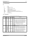
Table 4-3: Host Interface Pin Descriptions
Pin Name Type
PFBGA
Pin #
Cell
IO
Voltage
RESET
# State
Description