


Epson Research and Development Page 15
Vancouver Design Center
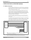
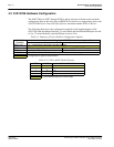
Connecting to a Micro-Controller via the Indirect Interface S1D13708
Issue Date: 01/12/12 X39A-G-020-01
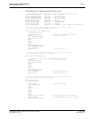
4.3 Register/Memory Mapping
When the S1D13708 is in Indirect mode it is not a memory mapped device. It uses the
protocol of first placing the register address on the data lines, then setting the register data
on the data lines for the next cycle. The data lines are a multipurpose data bus, they can
contain either the register address or the register data. The type of cycle, register address
(command) or register data (data), is controlled by the A0 command signal.
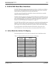
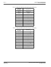
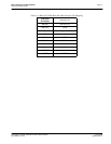
The 80K byte display buffer memory of the S1D13708 is accessed through the use of four
dedicated register sets. Registers REG[C0h], REG[C1h] and REG[C2h] contain the address
of the memory pointer, and register REG[C4h] is the ‘start’ register. To access memory,
REG[C2h], REG[C1h] and REG[C0h] are written with the desired memory address. Then,
a command access to register REG[C3h] will start the memory access. Subsequent
read/write data accesses will access the memory. The memory pointer address is automat-
ically incremented after a memory data access.
The overhead for reading a large block of memory is the same as reading a small block of
memory. Reading a single byte of memory will still require setting three address registers
and a fourth access to the ‘start’ register.
For further information on the Indirect Interface bus cycles, please refer to the S1D13708
Hardware Functional Specification, document number X39A-A-001-xx.