


Page 16 Epson Research and Development
Vancouver Design Center
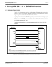
S1D13708 Interfacing to the Intel StrongARM SA-1110 Microprocessor
X39A-G-019-01 Issue Date: 01/11/25
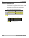
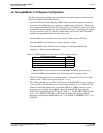
4.4 Register/Memory Mapping
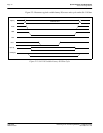
The S1D13708 is a memory-mapped device. The SA-1110 uses the memory assigned to a
chip select (nCS4 in this example) to map the S1D13708 internal registers and display
buffer. The S1D13708 uses two 128K byte blocks which are selected using A17 from the
SA-1110 (A17 is connected to the S1D13708 M/R# pin).The internal registers occupy the
first 128K bytes block and the 80K byte display buffer occupies the second 128K byte
block.
Each variable-latency IO chip select is assigned 128M Bytes of address space. Therefore;
if nCS4 is used the S1D13708 registers will be located at 4000 0000h and the display buffer
will be located at 4002 0000h. These blocks are aliased over the entire 128M byte address
space.
Note
If aliasing is not desirable, the upper addresses must be fully decoded.