


Epson Research and Development Page 41
Vancouver Design Center
Hardware Functional Specification S1D13708
Issue Date: 02/03/07 X39A-A-001-02
5 D.C. Characteristics
Note
When applying Supply Voltages to the S1D13708, Core V
DD
must be applied to the
chip before, or simultaneously with IO V
DD
, or damage to the chip may result.
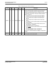
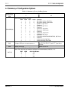
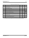
Table 5-1: Absolute Maximum Ratings (Preliminary - Subject to Change)
Symbol Parameter Rating Units
Core V
DD
Supply Voltage V
SS
- 0.3 to 4.0 V
IO V
DD
Supply Voltage V
SS
- 0.3 to 4.0 V
V
IN
Input Voltage V
SS
- 0.3 to IO V
DD
+ 0.5 V
V
OUT
Output Voltage V
SS
- 0.3 to IO V
DD
+ 0.5 V
T
STG
Storage Temperature -65 to 150 ° C
T
SOL
Solder Temperature/Time 260 for 10 sec. max at lead ° C
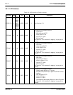
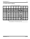
Table 5-2: Recommended Operating Conditions
Symbol Parameter Condition Min Typ Max Units
Core V
DD
Supply Voltage V
SS
= 0 V 1.62 1.8 1.98 V
IO V
DD
Supply Voltage V
SS
= 0 V 3.0 3.3 3.6 V
V
IN
Input Voltage V
SS
IO V
DD
V
T
OPR
Operating Temperature 0 70 ° C
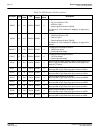
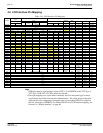
Table 5-3: Electrical Characteristics for VDD = 3.3V typical
Symbol Parameter Condition Min Typ Max Units
I
DDS
Quiescent Current Quiescent Conditions 170 µA
I
IZ
Input Leakage Current -1 1 µA
I
OZ
Output Leakage Current -1 1 µA
V
OH
High Level Output Voltage
VDD = min.
I
OH
= -8mA
V
DD
- 0.4 V
V
OL
Low Level Output Voltage
VDD = min.
I
OL
= 8mA
0.4 V
V
IH
High Level Input Voltage LVTTL Level, V
DD
= max 2.0 V
V
IL
Low Level Input Voltage LVTTL Level, V
DD
= min 0.8 V
V
T+
High Level Input Voltage LVTTL Schmitt 1.1 2.4 V
V
T-
Low Level Input Voltage LVTTL Schmitt 0.6 1.8 V
V
H1
Hysteresis Voltage LVTTL Schmitt 0.1 V
R
PD
Pull Down Resistance V
I
= V
DD
20 50 120 kΩ
C
I
Input Pin Capacitance 10 pF
C
O
Output Pin Capacitance 10 pF
C
IO
Bi-Directional Pin Capacitance 10 pF