


Epson Research and Development Page 9
Vancouver Design Center
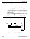
Interfacing to the NEC VR4181A™ Microprocessor S1D13708
Issue Date: 01/11/05 X39A-G-008-01
2.1.2 LCD Memory Access Signals
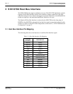
The S1D13708 requires an addressing range of 256K bytes. When the VR4181A external
LCD controller chip select signal is programmed to a window of that size, the S1D13708
resides in the VR4181A physical address range of 133C 0000h to 133F FFFFh. This range
is part of the external ISA memory space.
The following signals are required to access an external LCD controller. All signals obey
ISA signalling rules.
• A[16:0] is the address bus.
• #UBE is the high byte enable (active low).
• #LCDCS is the chip select for the S1D13708 (active low).
• D[15:0] is the data bus.
• #MEMRD is the read command (active low).
• #MEMWR is the write command (active low).
• #MEMCS16 is the acknowledge for 16-bit peripheral capability (active low).
• IORDY is the ready signal from S1D13708.
• SYSCLK is the prescalable bus clock (optional).
Once an address in the LCD block of memory is accessed, the LCD chip select (#LCDCS)
is driven low. The read or write enable signals (#MEMRD or #MEMWR) are driven low
for the appropriate cycle and IORDY is driven low by the S1D13708 to insert wait states
into the cycle. The high byte enable (UBE#) is driven low for 16-bit transfers and high for
8-bit transfers.