


Epson Research and Development Page 37
Vancouver Design Center
Hardware Functional Specification S1D13708
Issue Date: 02/03/07 X39A-A-001-02
4.3.3 Clock Input
4.3.4 Miscellaneous
4.3.5 Power And Ground
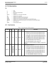
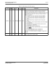
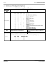
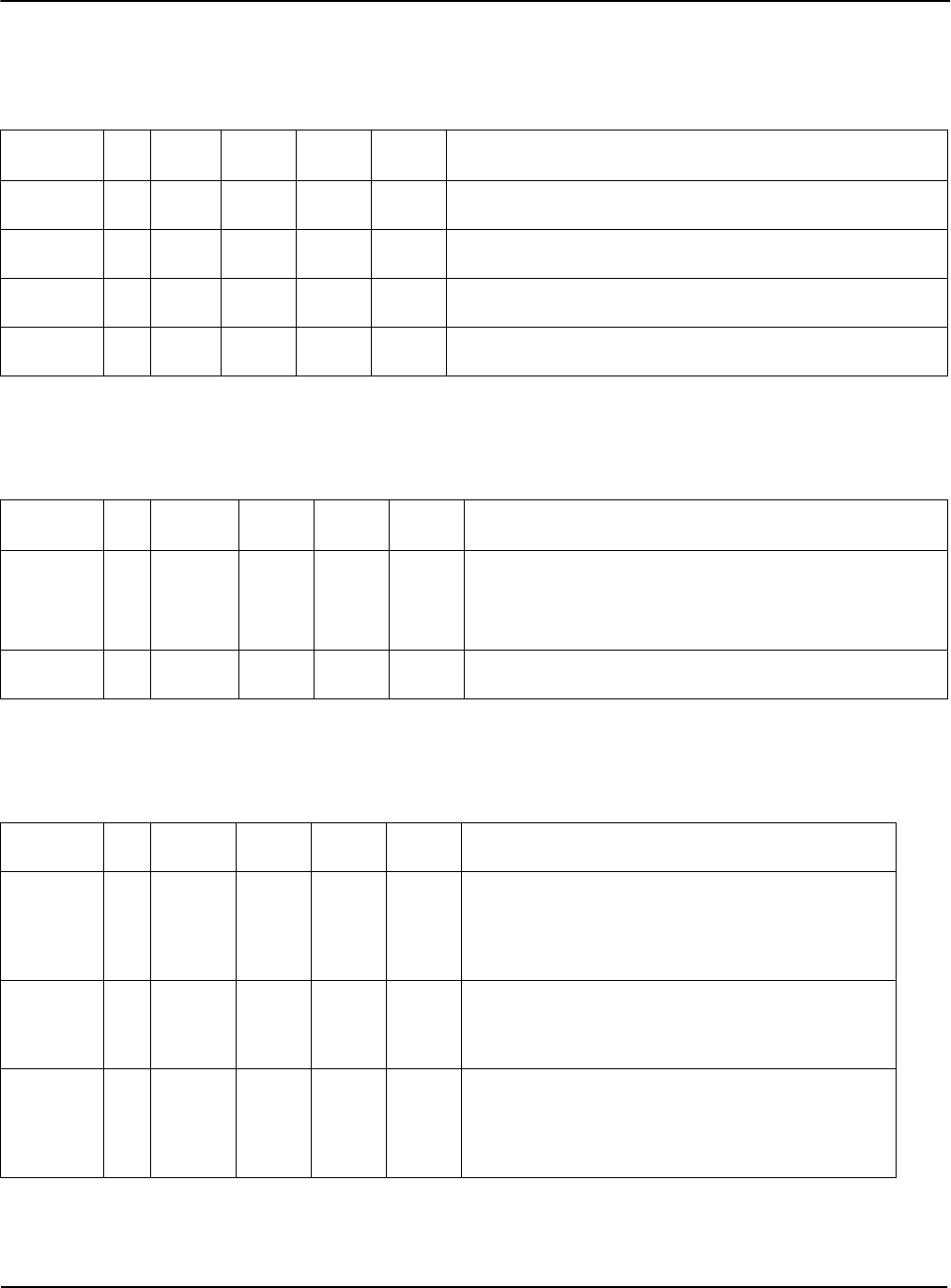
Table 4-5: Clock Input Pin Descriptions
Pin Name Type
PFBGA
Pin #
Cell
IO
Voltage
RESET#
State
Description
CLKI I F2 PCLK1 IOVDD —
Typically used as input clock source for bus clock and memory
clock.
CLKI2 I G9 PCLK1 IOVDD —
Typically used as input clock source for pixel clock This pin must
be tied to V
SS
when a crystal is not used.
XTAL0 0 F3 POSC1 IOVDD —
Crystal output. This pin must be left unconnected when a crystal is
not used.
XTAL1 I G1 POSC1 IOVDD —
Crystal input. This pin must be tied to V
SS
when a crystal is not
used.
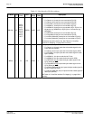
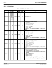
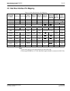
Table 4-6: Miscellaneous Pin Descriptions
Pin Name Type
PFBGA
Pin #
Cell
IO
Voltage
RESET#
State
Description
CNF[7:0] I
A9, B9,
B10, B11,
C10, C11,
D9, E8
PIC IOVDD —
These inputs are used to configure the S1D13708 - see Table
4-8: “Summary of Power-On/Reset Options,” on page 38.
Note: These pins are used for configuration of the
S1D13708 and must be connected directly to IO V
DD
or V
SS
.
TESTEN I D10 PIC IOVDD 0
Test Enable input used for production test only (has type 1 pull-
down resistor with a typical value of 50Ω at 3.3V).
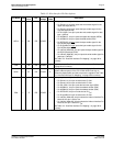
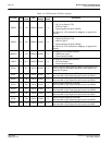
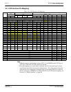
Table 4-7: Power And Ground Pin Descriptions
Pin Name Type
PFBGA
Pin #
Cell
IO
Voltage
RESET#
State
Description
IOVDD P
A1, A3,
A11, C7,
F11, G2,
K8,L2,
L11
P——IO V
DD
pins.
COREVDD P
A10, B1,
B5, F1,
H8, K5,
K11, L1
P——Core V
DD.
pins.
VSS P
E4, E5,
E6, E7,
F5, F7,
G5, G6,
G7
P——V
SS
pins.