


Epson Research and Development Page 11
Vancouver Design Center
Interfacing to the Motorola MC68VZ328 Dragonball Microprocessor S1D13708
Issue Date: 01/11/25 X39A-G-016-01
4 MC68VZ328 to S1D13708 Interface
4.1 Hardware Description
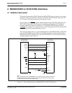
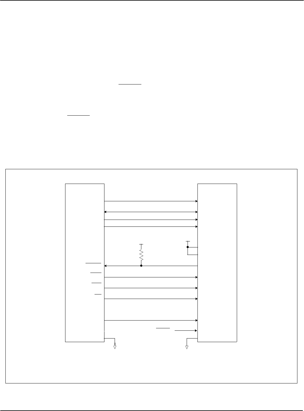
The interface between the S1D13708 and the MC68VZ328 does not requires any external
glue logic. Chip select module B is used to provide the S1D13708 with a chip select and
A17 is used to select between memory and register accesses.
In this example, the DTACK
signal is made available for the S1D13708. Alternately, the
S1D13708 can guarantee a maximum cycle length that the Dragonball VZ handles by
inserting software wait states (see Section 4.2.2, “MC68VZ328 Chip Select and Pin
Configuration” on page 13). A single resistor is used to speed up the rise time of the WAIT#
(DTACK
) signal when terminating the bus cycle.
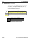
The following diagram shows a typical implementation of the MC68VZ328 to S1D13708
using the Dragonball host bus interface. For further information on the Dragonball Host
Bus interface and AC Timing, refer to the S1D13708 Hardware Functional Specification,
document number X39A-A-001-xx.
Figure 4-1: Typical Implementation of MC68VZ328 to S1D13708 Interface
MC68VZ328 S1D13708
A[16:0]
D[15:0]
DTACK
UWE
LWE
OE
CLK0
AB[16:0]
DB[15:0]
CS#
WAIT#
WE1#
WE0#
RD#
RD/WR#
CLKI
RESET#
IO V
DD
1K
CSB1
BS#
Note:
When connecting the S1D13708 RESET# pin, the system designer should be aware of all
conditions that may reset the S1D13708 (e.g. CPU reset can be asserted during wake-up
from power-down modes, or during debug states).
System RESET
IO V
DD
A17
M/R#