Epson Research and Development Page 191
Vancouver Design Center
Hardware Functional Specification S1D13708
Issue Date: 02/03/07 X39A-A-001-02
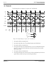
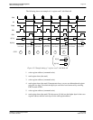
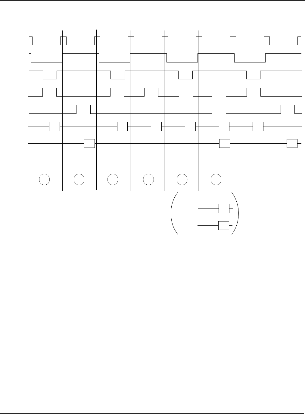
The following shows an example of a “register read” with Mode 68.
Figure 15-2 Sample timing of “register read” with Mode 68
1. write register address (command write).
2. read register data (data read).
3. write register address (command write).
4. read register data (data read). Demonstrates how to access an odd numbered register
using the low byte. Note that the high byte could also have been used by asserting
EBU instead of EBL.
5. write register address (command write).
6. read register data (data read). Word accesses (16-bit) use the higher byte for the even
register address and the lower byte for the odd register address.
A0
CS#
EBL
R/W#
EBU
D[7:0]
D[15:8]
CMD0 CMD1 CMD2 CMD4
DATA1
DATA0
DATA2
DATA3
DATA4
command write
even number odd number
data read
command write command write command write
even number even number
data read data read
data read
byte access byte access
word access byte access
1 2 3 4 5 6
DATA2
DATA3
Little Endian
D[7:0]
D[15:8]
(Big Endian)
STEP


