


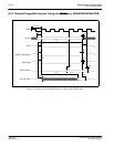
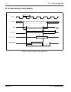
Epson Research and Development Page 55
Vancouver Design Center
Hardware Functional Specification S1D13708
Issue Date: 02/03/07 X39A-A-001-02
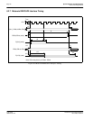
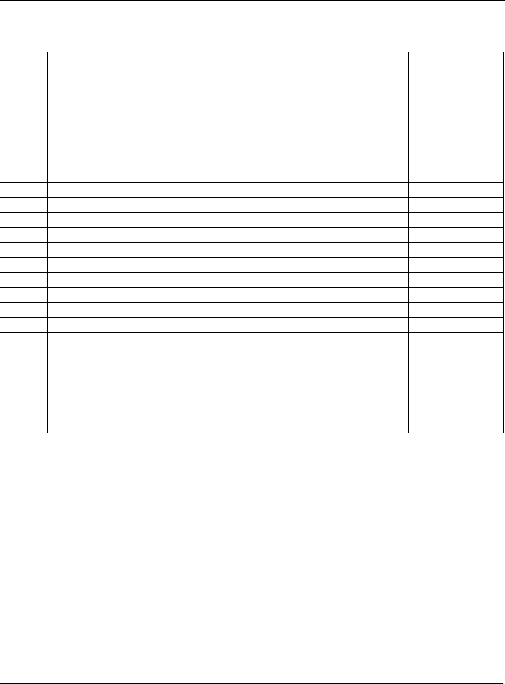
1. t17 is the delay from when data is placed on the bus until the data is latched into the write buffer.
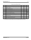
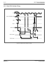
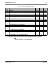
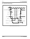
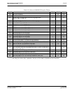
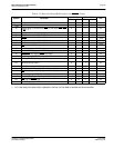
Table 6-10: Motorola MC68K #2 Interface Timing
Symbol Parameter Min Max Unit
f
CLK
Bus Clock frequency 50 MHz
T
CLK
Bus Clock period 1/f
CLK
ns
t3
A[16:0], SIZ[1:0], M/R# setup to first CLK rising edge where
CS# = 0, AS# = 0, DS# = 0
4ns
t4 A[16:0], SIZ[1:0], M/R#, R/W# hold from AS# rising edge 0 ns
t5 CS# setup to CLK rising edge 3 ns
t6 CS# hold from AS# rising edge 0 ns
t7a DSACK1# asserted for MCLK = BCLK 8 T
CLK
t7b DSACK1# asserted for MCLK = BCLK ÷ 213T
CLK
t7c DSACK1# asserted for MCLK = BCLK ÷ 317T
CLK
t7d DSACK1# asserted for MCLK = BCLK
÷ 422T
CLK
t8 AS# falling edge to CLK rising edge 4 ns
t9 AS# rising edge to CLK rising edge 4 ns
t10 DS# falling edge to CLK rising edge 4 ns
t11 DS# setup to CLK rising edge 4 ns
t12 First CLK where AS# = 1 to DSACK1# high impedance 2 28 ns
t13 R/W# setup to CLK rising edge before all CS# = 0, AS# = 0, and DS# = 0 1 ns
t15 AS# = 0 and CS# = 0 to DSACK1# rising edge 3 10 ns
t16 AS# rising edge to DSACK1# rising edge 5 14 ns
t17
D[31:16] valid to third CLK rising edge where CS# = 0, AS# = 0, and DS# = 0
(write cycle) (see note 1)
1ns
t18 D[31:16] hold from falling edge of DSACK1# (write cycle) 0 ns
t19 DS# falling edge to D[31:16] driven (read cycle) 5 14 ns
t20 DSACK1# falling edge to D[31:16] valid (read cycle) 0 ns
t21 DS# rising edge to D[31:16] invalid/high impedance (read cycle) 3 10 ns