


Page 194 Epson Research and Development
Vancouver Design Center
S1D13708 Hardware Functional Specification
X39A-A-001-02 Issue Date: 02/03/07
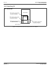
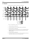
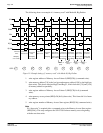
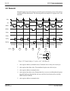
The following shows an example of a “memory read” with Mode 68, Big Endian.
Figure 15-4 Sample timing of “memory read” with Mode 68, Big Endian
1. write register address of Memory Access Pointer 0 (REG[C0h]) (command write).
2. write memory address[7:0] to the low byte and memory address[15:8] to the high byte
(data write). This places data into RegC0 and RegC1, which form bits [7:0] and [15:8]
of memory address respectfully.
3. write register address of Memory Access Pointer 2 (REG[C2h] bit 0) (command
write).
4. write memory access pointer (REG[c2h] bit 0) (data write). This forms bit 16 of mem-
ory address.
5. write register number of Memory Access Start register (REG[C4h] (command write).
Note
No “data write” is required after a command write to the Memory Access Start register
(REG[C4h]). This step configures the S1D13708 for burst memory access beginning
with the next data write.
A0
CS#
EBL
R/W#
EBH
D[7:0]
D[15:8]
REG[C0h]
Data Write
word access
Command
Data Write
byte access
even number
memory data
Data Read
Data Read
Data Read Data Read Data Read
byte access
word access
word access
memory data
memory data memory data
Address +2
byte access
byte access
memory data
odd address
even address
odd address even address
even address
Write
Command
Write
Command
Write
REG[C4h]
REG[C2h]
even number
(word)
Address +2
(word)
Address +1
(byte)
Address +1
(byte)
1 2 3 4 5 6 6 6 6 6
STEP